
Mathis on Graphene? Any hints?
Page 4 of 4 •  1, 2, 3, 4
Re: Mathis on Graphene? Any hints?
![]() by Chromium6 Sat Jan 14, 2023 2:31 am
by Chromium6 Sat Jan 14, 2023 2:31 am
Can a British startup solve concrete's perilous environmental problem?
January 11, 2023 - 7:50 pm
Concrete has been described as the most destructive material on Earth. After water, it’s the most used substance in the world, with twice the usage of steel, wood, plastics, and aluminium combined.
To manufacture all this concrete, more than 4 billion tonnes of cement are produced every year. According to the Chatham House think tank, that creates around 8% of all CO2 emissions — more than what’s caused by all the trucks across the globe.
Cement makers urgently need to reduce this footprint. To meet the requirements of the Paris Agreement on climate change, the industry needs to cut emissions by at least 16% by 2030. At the same time, the sector faces growing demand from rapid urbanization and population growth.
Get your tickets for TNW Valencia in March!
The heart of tech is coming to the heart of the Mediterranean
It’s foreboding problem. But engineers believe that graphene offers a solution.
“Just 0.01% of the material is required.
First isolated at the University of Manchester in 2004, Graphene’s 2D nature provides a unique combination of strength, flexibility, lightness, and conductivity. These properties caught the eye of Nationwide Engineering, a British construction business.
The firm’s memorably-acronymed R&D subsidiary, NERD (Nationwide Engineering Research and Development), was tasked with turning the “wonder material” into a new additive: Concretene.
Amesbury pour - hi-res
The substance has already formed floor slabs in the UK. Credit: Concretene
Concretene consists of graphene that’s produced at Manchester University. Small quantities of the liquid formulation are added during the concrete mixing process.
The graphene provides both mechanical support and an active surface for the chemical reactions that occur during the cement hydration and hardening.
“Very low dosages of the material, in some cases less than 0.01%, are required to deliver substantial performance gains,” Alex McDermott, the co-founder of Concretene, tells TNW.
“This means that Concretene is commercially viable with wholesale costs to be in-line with existing additives already used in the concrete industry.”
According to McDermott, Concretene used in real construction projects was up to 30-50% stronger than standard concrete. Subsequent lab tests have shown strength gains that surpass 100%. As a result, the volume of cement required can significantly reduce without impairing performance.
Costs, shrinking, and cracking can also be trimmed, while increases in density cut concrete’s porosity.
“These factors will enable engineers to reduce the volume of concrete required in designs going forward, further reducing the CO₂ impact,” says McDermott.
Ultimately, he believes Concretene could be used in more than 99% of concretes worldwide.
McDermott, Concretene
McDermott’s team worked with the University of Manchester’s Graphene Engineering Innovation Centre (GEIC) to develop Concretene. Credit: Concretene
Initial tests of Concretene have produced promising results.
In 2021, NERD laid the world’s first graphene concrete slab across the floor of a new gym in England. Further trials followed at a roller disco and a residential development.
In total, more than 1,000 tonnes of Concretene have now been poured in real-world projects. The next target is pushing the product into the mainstream.
more at link: https://thenextweb.com/news/concretene-uses-graphene-reduce-concrete-carbon-footprint
Chromium6- Posts : 727
Join date : 2019-11-29
Re: Mathis on Graphene? Any hints?
![]() by Chromium6 Sat Jan 14, 2023 2:41 am
by Chromium6 Sat Jan 14, 2023 2:41 am
http://milesmathis.com/graphene.pdf
331b. Graphene. Where we see all the mainstream explanations are wrong. Why? Because they are based on electron bonding theory, which is a fudge from the first word. 10pp.
------------
Articles
Is Graphene Really a 2D Material?
Is Graphene Two-Dimensional?
In 2010 the Nobel committee awarded the Prize in Physics to Andre Geim and Konstantin Novoselov “for ground breaking experiments regarding the two-dimensional material graphene”. However the debate about the real dimensionality of graphene is still open: Is it two or three-dimensional? “Some of the debate surrounds the observation that the graphene sheets are not perfectly flat but can contain waves as distortions since the carbon rings are puckered”, explains Professor Samantha Jenkins, College of Chemistry and Chemical Engineering, Hunan Normal University, China.
Euclidean Geometry
From Euclidean geometry a graphene sheet oriented in the 3-D Cartesian x-y plane is defined as being three-dimensional. This is because such a sheet has a finite extent along the x-, y- and z-Cartesian axes. Due to their “thickness” the carbon atoms have a finite extent along the z-axis, and also the sheet may contain wave-like features creating displacements of the graphene sheet along the z-axis.
Within Euclidean geometry there is the assumption that a three dimensional object will always remain three-dimensional no matter how small it is. Euclidean geometry, however, takes no account of the quantum nature of matter at the nanoscale, which renders all materials granular by virtue of having atoms as the building blocks.
For Samantha Jenkins “it became apparent that the judgment one was making on the morphology of a molecule was based purely on experience with everyday macroscopic objects”. She thinks this is surely not appropriate for these quantum mechanical objects. Looking at the topology of the electron density can be a more efficient way.
Quantum Theory of Atoms In Molecules (QTAIM)
The framework of the Quantum Theory of Atoms In Molecules (QTAIM), originated by the late Canadian chemist Richard F. W. Bader, partitions such a distribution so there are no gaps between the atoms. And it defines special points – so called ‘critical points’ – where the gradient of the total charge density distribution is zero.
“Imagine a topographic map of a landscape with contours to represent the topology of the landscape in terms of the elevation”, says Jenkins. “The highest points on such a map are, of course, the mountain peaks where the contour lines are very closely spaced. At the bottom of wide and flat valleys the contours are very widely spaced”. In this picture, mountain peaks are compared to the nuclear positions of atoms in molecules since they have the highest local values of the charge density, thus defining ‘nuclear critical points’ (NCPs). The bottoms of the valleys can be compared to the regions, for instance, at the center of the rings in the graphene structure. Here the charge density will be a minimum, defining ‘ring critical points’ (RCPs). The path between two mountain peaks, forming a saddle shape through the lowest point between them, can be compared with the bonds in a material, or ‘bond critical points’ (BCP). Another type of critical point, the ‘cage critical point’ or CCP is a local minimum with electron density rising in all three directions of space. CCPs are located, e.g., at the geometric center of a C60 molecule. It is now easy to see how the collective set of critical points in QTAIM, along with the network of bonds, called a ‘molecular graph’, can become a powerful tool in the non-trivial past of determining the morphologies of solids, clusters, and molecules.
The presence of a CCP is, therefore, necessary for the molecule or material to be describable as “quantum topologically” in 3 dimensions, or 3-DQT. Further to this, it is easy to see that for a molecular graph the existence of a ring critical point, RCP, is necessary to be classed as having 2-DQT geometry. Similarly then, a molecular graph with no cage, CCP, or ring critical points, RCP, would be 1-DQT. The last observation was that isolated atoms only contain nuclear critical points, NCP, and are, therefore, 0-DQT.
To Settle the Debate
QTAIM can now settle the debate about whether the graphene sheet is two or three dimensional from a quantum mechanical viewpoint. The molecular graphs of graphene sheets contain nuclear, NCP, bond, BCP, and ring critical points, RCP, but no cage critical points, CCP, so the quantum geometry is quantified as being 2-DQT and not 3-DQT.
“This means that the Nobel committee was, in a way, correct in stating that the geometry of graphene is describable as two dimensional, although their judgment was not based on quantum mechanics of all of the electrons and nuclei, but on the conduction behavior of some of the electrons”, concludes Jenkins.
Quantum topology phase diagrams for molecules, clusters, and solids,
Samantha Jenkins,
Int. J. Quantum Chem. 2013, 113 (11), 1603–1608.
DOI: 10.1002/qua.24398
87th Annual Meeting of the Israel Chemical Society (ICS)
July 4, 2023 to July 5, 2023
7th International Congress on Operando Spectroscopy
May 7, 2023 to May 11, 2023
Thermochemical Energy Storage (TCES)
January 3, 2023
New President of the Italian Chemical Society
Quantum topology phase diagrams for molecules, clusters, and solids,
Samantha Jenkins,
Int. J. Quantum Chem. 2013, 113 (11), 1603–1608.
DOI: 10.1002/qua.24398
http://onlinelibrary.wiley.com/doi/10.1002/qua.24398/abstract
Chromium6- Posts : 727
Join date : 2019-11-29
Re: Mathis on Graphene? Any hints?
![]() by Chromium6 Sat Jan 14, 2023 2:51 am
by Chromium6 Sat Jan 14, 2023 2:51 am
https://polymer-additives.specialchem.com/tech-library/article/graphene-2d-materials-technology-and-market-update
Structure of Molybdenum Disulphide (L) and Tungsten Ditelluride (R)
Molybdenum Disulphide (MoS2) (L), Tungsten Ditelluride (WTe2) (R)
Bulk TMDCs are van der Waals materials with each layer being three atoms thick, consisting of the metal layer sandwiched between two chalcogenide layers. TMDCs are finding use in semiconductor manufacturing systems where abrasion-resistant, electrically conductive surface materials are required.
Phosphorene —
It is a single layer of black phosphorus, a layered, stable variation of elemental phosphorus. It is a direct bandgap semiconductor with a puckered honeycomb structure. The bandgap can be tuned throughout the visible region by stacking layers on top of each other. It has good charge mobility, therefore making it suitable for optoelectronic devices and transistors.
Phosphorene or 2D Black Phosphorus Honeycomb Structure
Xenes —
Monolayers of silicon, germanium, and tin are collectively known as Xenes and follow the graphene naming convention. They have a hexagonal structure similar to graphene but are buckled to varying degrees.
Buckled Hexagonal Xene Structures
Silicon (L), Germanium (C), Tin (R) Buckled Hexagonal Xene Structures
While still very much in their infancy, potential applications range from electric field-effect transistors to topological or surface tailored insulators. Recently bismuth Xenes are under development and show potential for magneto-electronic enclosure applications, particularly for military lightning strike protection.
2D Graphene Material Plastic Resin Systems
Graphene plastic resin system development is currently focused on by end-use product developers. They use an array of graphene material forms, such as:
Powders,
Flakes,
Nanoplatelets,
Nanoribbons, and
Lattice structures
Compounding techniques include:
Single and twin-screw compounding,
Dispersion,
Masterbatch,
Rubber banbury and continuous mixing,
Aqueous and solvent coating mixing,
Hot melt adhesive dispersion, and
Spray coating solutions
Vorbeck Materials Group’s Vor-x Graphene Sheet
Vorbeck Materials Group’s Vor-x, a proprietary form of graphene containing functional groups, represents a historically relevant as well as ongoing breakthrough entry into the conductive polymer additives market. The functionalized graphene allows compatibility to be ‘tuned’ to a specific plastic resin matrix, or allows specific material properties to be enhanced.
Vor-x graphene layers are entirely disassociated, and due to their wrinkled morphology, individual sheets do not reaggregate, ensuring good dispersion and handling. Compounding Vor-x masterbatches into plastics is much less difficult than a 1D Carbon NanoTube (CNT) masterbatch material. Vor-x yields conductivities well beyond anti-static and into the conductive range.
https://polymer-additives.specialchem.com/tech-library/article/graphene-2d-materials-technology-and-market-update
---------------
Looks like this is of high interest since a lot of "investment" money is in play...hope Miles gets a citation or at least a mention:
https://graphene-conference.com/index
The Premier Forum for Industrial Applications for Graphene & 2D Materials
Welcome to the Graphene & 2D Materials 2023, where nanomaterials researchers and industry leaders will meet in Los Angeles, California, to explore new graphene-based solutions for use in industrial applications.
Graphene, an ultra-lightweight and solid material, is 200 times stronger than steel, incredibly thin and flexible, a superb conductor, and can offer a solid barrier. As the production and processing of graphene have advanced, manufacturers are eager to establish supplies, integrate graphene into existing processes, and explore new uses of graphene in a multitude of industry applications, including electronics, thermal management, and structural uses.
While graphene is emerging as the most promising nanomaterial because of its unique combination of superb properties, industries face several critical challenges before wide-scale commercial use can be established. The solution for the commercialization lies in the standardization of high- quality materials in a scalable manner, developments in material integration and processes, and the production of graphene at the lowest possible cost to achieve profitable applications.
This year’s Graphene & 2D Materials 2023 event is set to become the world’s leading exhibition and conference exclusively for graphene researchers and industry leaders to meet and explore new uses of graphene in industrial products and to address the specific challenges associated with the commercialization of graphene for use in a multitude of new applications.
Key topics on this year’s agenda include:
Graphene availability, market supply, and demand forecasts
New markets and the commercialization of graphene in industrial applications
Quality and standardization of graphene materials to meet commercial needs
New developments in manufacturing processes and material integration techniques
Latest methods, results, and new developments in 2D materials and composites
End-user industrial manufacturer case studies and successful applications
This exhibition and conference will provide a forum for all stakeholders, from researchers and suppliers in the graphene industry to end-user manufacturers, to network and build cross-market relationships and discuss the latest developments in graphene use in new industrial applications.
Call for Presentation
If you would like to be a speaker at this event, please contact sean.collins@iQ-Hub.com, subject heading “Call for Papers – Graphene & 2D Materials 2023”
To secure your place at Graphene & 2D Materials 2023 or if you require more information, please contact delegates@iQ-Hub.com.
https://player.vimeo.com/video/236701630
Featured Speakers
Jon Taylor
NeoGraf
Cory Doble
Martinrea International US Inc
Haley Marie Keith
MITO Material Solutions Inc
--------------------
Graphene Going Forward
Graphene 2DGraphene's unique 2D structure means that electrons travel through it differently compared to most other materials via a so-called atomic brick structure. One consequence of this unique transport phenomena is that applying a voltage to them, doesn't stop the electrons as in most other materials. To make useful applications out of graphene and its unique electrons for quantum computer development, it is critical to be able to tailor stop and control graphene electrons mechanisms within its atomic brick structure.
Food Freshness SensorGraphene sensors have been tuned to monitor food freshness and safety. Researchers tailored their new, printed on PET (PolyEthylene Terephthalate) sensors into tuna broth and monitored the readings. It turned out the sensors printed with high-resolution aerosol jet printers on a flexible polymer film and tuned to test for histamine, an allergen and indicator of spoiled fish and meat can detect histamine down to 3.41 parts per million.
George H. Luh GraphCOND LED Lighting Bulb BaseGerman company Georg H. Luh is a market leader in TC mineral additive products for heat management. Their technology is based on graphene nanoplatelets that enhance not only thermal but also electrical conductivity. There are two base grades namely:
GraphTHERM
GraphCOND
These technologies are very useful for energy efficient, long duration LED (Light Emitting Diode) bulb bases.
Check Out the Commercially Available Graphene / Graphene Oxides
More at link: https://polymer-additives.specialchem.com/tech-library/article/graphene-2d-materials-technology-and-market-update
Last edited by Chromium6 on Sat Jan 14, 2023 3:33 am; edited 1 time in total
Chromium6- Posts : 727
Join date : 2019-11-29
Re: Mathis on Graphene? Any hints?
![]() by Chromium6 Sat Jan 14, 2023 3:02 am
by Chromium6 Sat Jan 14, 2023 3:02 am
http://milesmathis.com/pauli.pdf (mentions photon reflections)
https://www.mediafire.com/file/gqgrym9grpke1hw/MoS.xlsx/file
------------
https://en.wikipedia.org/wiki/Molybdenum_disulfide
Molybdenum disulfide (or moly) is an inorganic compound composed of molybdenum and sulfur. Its chemical formula is MoS2.
The compound is classified as a transition metal dichalcogenide. It is a silvery black solid that occurs as the mineral molybdenite, the principal ore for molybdenum.[6] MoS2 is relatively unreactive. It is unaffected by dilute acids and oxygen. In appearance and feel, molybdenum disulfide is similar to graphite. It is widely used as a dry lubricant because of its low friction and robustness. Bulk MoS2 is a diamagnetic, indirect bandgap semiconductor similar to silicon, with a bandgap of 1.23 eV.[2] Single layer sheets act as a perfect mirror, reflecting 100% of incident photons.[7]
..........
Lubricant
A tube of commercial graphite powder lubricant with molybdenum disulfide additive (called "molybdenum")[34]
Due to weak van der Waals interactions between the sheets of sulfide atoms, MoS2 has a low coefficient of friction. MoS2 in particle sizes in the range of 1–100 µm is a common dry lubricant.[35] Few alternatives exist that confer high lubricity and stability at up to 350 °C in oxidizing environments. Sliding friction tests of MoS2 using a pin on disc tester at low loads (0.1–2 N) give friction coefficient values of <0.1.[36][37]
MoS2 is often a component of blends and composites that require low friction. For example, it is added to graphite to improve sticking.[34] A variety of oils and greases are used, because they retain their lubricity even in cases of almost complete oil loss, thus finding a use in critical applications such as aircraft engines. When added to plastics, MoS2 forms a composite with improved strength as well as reduced friction. Polymers that may be filled with MoS2 include nylon (trade name Nylatron), Teflon and Vespel. Self-lubricating composite coatings for high-temperature applications consist of molybdenum disulfide and titanium nitride, using chemical vapor deposition.
Examples of applications of MoS2-based lubricants include two-stroke engines (such as motorcycle engines), bicycle coaster brakes, automotive CV and universal joints, ski waxes[38] and bullets.[39]
Other layered inorganic materials that exhibit lubricating properties (collectively known as solid lubricants (or dry lubricants)) includes graphite, which requires volatile additives and hexagonal boron nitride.[40]

Related Japanese research: https://milesmathis.forumotion.com/t262-japan-tokai-university-found-a-room-temperature-superconductor-with-critical-temperature-near-the-melting-point-of-tin?highlight=Super+critical
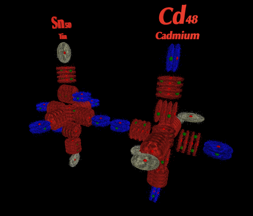
Reference for Miles' structures: https://milesmathis.forumotion.com/t51-mathis-chemistry-graphics
Tin Superconductors mentioned in this thread:


Chromium6- Posts : 727
Join date : 2019-11-29
Re: Mathis on Graphene? Any hints?
![]() by Chromium6 Sun Jan 22, 2023 12:53 am
by Chromium6 Sun Jan 22, 2023 12:53 am
------------
NEWS RELEASE 13-AUG-2015
Black phosphorus surges ahead of graphene
A Korean team of scientists tune BP's band gap to form a superior conductor, allowing for the application to be mass produced for electronic and optoelectronics devices
Peer-Reviewed Publication
INSTITUTE FOR BASIC SCIENCE
Graphene - The Would be King of 2-D Materials
IMAGE: THE RESEARCH TEAM OPERATING OUT OF POHANG UNIVERSITY OF SCIENCE AND TECHNOLOGY, AFFILIATED WITH THE INSTITUTE FOR BASIC SCIENCE'S CENTER FOR ARTIFICIAL LOW DIMENSIONAL ELECTRONIC SYSTEMS, REPORTED A TUNABLE BAND GAP IN BP, EFFECTIVELY MODIFYING THE SEMICONDUCTING MATERIAL INTO A UNIQUE STATE OF MATTER WITH ANISOTROPIC DISPERSION. THIS RESEARCH OUTCOME POTENTIALLY ALLOWS FOR GREAT FLEXIBILITY IN THE DESIGN AND OPTIMIZATION OF ELECTRONIC AND OPTOELECTRONIC DEVICES LIKE SOLAR PANELS AND TELECOMMUNICATION LASERS. view more
CREDIT: INSTITUTE FOR BASIC SCIENCE
- A Korean team of scientists tune BP's band gap to form a superior conductor, allowing for the application to be mass produced for electronic and optoelectronics devices
The research team operating out of Pohang University of Science and Technology (POSTECH), affiliated with the Institute for Basic Science's (IBS) Center for Artificial Low Dimensional Electronic Systems (CALDES), reported a tunable band gap in BP, effectively modifying the semiconducting material into a unique state of matter with anisotropic dispersion. This research outcome potentially allows for great flexibility in the design and optimization of electronic and optoelectronic devices like solar panels and telecommunication lasers.
To truly understand the significance of the team's findings, it's instrumental to understand the nature of two-dimensional (2-D) materials, and for that one must go back to 2010 when the world of 2-D materials was dominated by a simple thin sheet of carbon, a layered form of carbon atoms constructed to resemble honeycomb, called graphene. Graphene was globally heralded as a wonder-material thanks to the work of two British scientists who won the Nobel Prize for Physics for their research on it.
Graphene is extremely thin and has remarkable attributes. It is stronger than steel yet many times lighter, more conductive than copper and more flexible than rubber. All these properties combined make it a tremendous conductor of heat and electricity. A defect-free layer is also impermeable to all atoms and molecules. This amalgamation makes it a terrifically attractive material to apply to scientific developments in a wide variety of fields, such as electronics, aerospace and sports. For all its dazzling promise there is however a disadvantage; graphene has no band gap.
Stepping Stones to a Unique State
A material's band gap is fundamental to determining its electrical conductivity. Imagine two river crossings, one with tightly-packed stepping-stones, and the other with large gaps between stones. The former is far easier to traverse because a jump between two tightly-packed stones requires less energy. A band gap is much the same; the smaller the gap the more efficiently the current can move across the material and the stronger the current.
Graphene has a band gap of zero in its natural state, however, and so acts like a conductor; the semiconductor potential can't be realized because the conductivity can't be shut off, even at low temperatures. This obviously dilutes its appeal as a semiconductor, as shutting off conductivity is a vital part of a semiconductor's function.
Birth of a Revolution
Phosphorus is the fifteenth element in the periodic table and lends its name to an entire class of compounds. Indeed it could be considered an archetype of chemistry itself. Black phosphorus is the stable form of white phosphorus and gets its name from its distinctive color. Like graphene, BP is a semiconductor and also cheap to mass produce. The one big difference between the two is BP's natural band gap, allowing the material to switch its electrical current on and off. The research team tested on few layers of BP called phosphorene which is an allotrope of phosphorus.
Keun Su Kim, an amiable professor stationed at POSTECH speaks in rapid bursts when detailing the experiment, "We transferred electrons from the dopant - potassium - to the surface of the black phosphorus, which confined the electrons and allowed us to manipulate this state. Potassium produces a strong electrical field which is what we required to tune the size of the band gap."
This process of transferring electrons is known as doping and induced a giant Stark effect, which tuned the band gap allowing the valence and conductive bands to move closer together, effectively lowering the band gap and drastically altering it to a value between 0.0 ~ 0.6 electron Volt (eV) from its original intrinsic value of 0.35 eV. Professor Kim explained, "Graphene is a Dirac semimetal. It's more efficient in its natural state than black phosphorus but it's difficult to open its band gap; therefore we tuned BP's band gap to resemble the natural state of graphene, a unique state of matter that is different from conventional semiconductors."
The potential for this new improved form of black phosphorus is beyond anything the Korean team hoped for, and very soon it could potentially be applied to several sectors including engineering where electrical engineers can adjust the band gap and create devises with the exact behavior desired. The 2-D revolution, it seems, has arrived and is here for the long run.
###
JOURNAL
Science
Disclaimer: AAAS and EurekAlert! are not responsible for the accuracy of news releases posted to EurekAlert! by contributing institutions or for the use of any information through the EurekAlert system.
Media Contact
Sunny Kim
Institute for Basic Science
sunnykim@ibs.re.kr
Office: 82-428-788-135
More on this News Release
Black phosphorus surges ahead of graphene
INSTITUTE FOR BASIC SCIENCE
JOURNAL
Science
FUNDER
Institute for Basic Science
KEYWORDS
BAND GAPGRAPHENEELECTRON TRANSFER
ADDITIONAL MULTIMEDIA
https://www.eurekalert.org/news-releases/886830
--------------------
Also:
https://fuelcellsworks.com/news/first-graphene-turns-petroleum-into-graphite-and-green-hydrogen/
Chromium6- Posts : 727
Join date : 2019-11-29
Re: Mathis on Graphene? Any hints?
![]() by Chromium6 Sun Jan 22, 2023 12:58 am
by Chromium6 Sun Jan 22, 2023 12:58 am
----------
Researchers turn waste byproduct asphaltene into graphene
Researchers from Rice University, University of Calgary, South Dakota School of Mines and Technology and University of Washington have managed to turn a waste material called asphaltene (a byproduct of crude oil production) into graphene.
Image
Schematic conceptualization of sustainable valorization of asphaltene image
Rice University's Muhammad Rahman, an assistant research professor of materials science and nanoengineering, is employing Rice’s unique flash Joule heating process to convert asphaltenes instantly into turbostratic (loosely aligned) graphene and mix it into composites for thermal, anti-corrosion and 3D-printing applications. The process makes good use of material otherwise burned for reuse as fuel or discarded into tailing ponds and landfills. Using at least some of the world’s reserve of more than 1 trillion barrels of asphaltene as a feedstock for graphene would be good for the environment as well.
“Asphaltene is a big headache for the oil industry, and I think there will be a lot of interest in this,” said Rahman, who characterized the process as both a scalable and sustainable way to reduce carbon emissions from burning asphaltene.
Asphaltenes are 70% to 80% carbon already. The Rice lab combines it with about 20% of carbon black to add conductivity and flashes it with a jolt of electricity, turning it into graphene in less than a second. Other elements in the feedstock, including hydrogen, nitrogen, oxygen and sulfur, are vented away as gases.
“We try to keep the carbon black content as low as possible because we want to maximize the utilization of asphaltene,” Rahman said.
“The government has been putting pressure on the petroleum industries to take care of this,” said Rice graduate student and co-lead author M.A.S.R. Saadi. “There are billions of barrels of asphaltene available, so we began working on this project primarily to see if we could make carbon fiber. That led us to think maybe we should try making graphene with flash Joule heating.”
Assured that Professor James Tour’s process worked as well on asphaltene as it did on various other feedstocks, including plastic, electronic waste, tires, coal fly ash and even car parts, the researchers set about making things with their graphene. Saadi, who works with Rahman and Ajayan, mixed the graphene into composites, and then into polymer inks bound for 3D printers. “We’ve optimized the ink rheology to show that it is printable,” he said, noting the inks have no more than 10% of graphene mixed in. Mechanical testing of printed objects is forthcoming, he said.
Source:
Science Advances eurekalert
Tags:
Graphene applications Graphene composites Technical / Research Rice University
Posted: Nov 19,2022 by Roni Peleg
https://www.graphene-info.com/researchers-turn-waste-byproduct-asphaltene-graphene
Chromium6- Posts : 727
Join date : 2019-11-29
Re: Mathis on Graphene? Any hints?
![]() by Lloyd Mon Feb 27, 2023 12:26 pm
by Lloyd Mon Feb 27, 2023 12:26 pm
Boosting superconductivity in graphene bilayers [Why? to make deadlier vaxes?]
https://phys.org/news/2023-02-boosting-superconductivity-graphene-bilayers.html
Lloyd- Posts : 166
Join date : 2022-04-12
Chromium6 likes this post
Re: Mathis on Graphene? Any hints?
![]() by Chromium6 Tue Feb 28, 2023 4:19 am
by Chromium6 Tue Feb 28, 2023 4:19 am
Lloyd wrote:Cr6, do you think there might be anything to my speculation?
Boosting superconductivity in graphene bilayers [Why? to make deadlier vaxes?]
https://phys.org/news/2023-02-boosting-superconductivity-graphene-bilayers.html
If it is from Rice Universtity...they are probably looking to boost Oil/Gas outputs from Oil/Gas companies in Houston. Asphaltene is a nasty output that could be "changed" for the better. I hate to think they gunned the vaxxes for using the body's charge field for infection. It is a bad thought. C-H bonding is kind of mysterious with the body's cells overall IMHO. The C.F. alignment per Miles with the body is the cure for a lot bad diseases...cancers primarily which does work with ATP-energy creation -- cancers basically grow where Oxygen usage-ATP-energy creation doesn't happen naturally -- cancers grow in these environments which can develop in people. Really look at "What causes a cancer cell to grow?"...it comes down to the charge field and the energy to power the cell growth... without the C.F. it goes undetected by T-Cells. Like why is radiation used as treatment? It simply reduces the C.F. and allows the body to pick up the infection-abnormal cells at a massive cellular cost. This is a big generalization but I think it is true. Most cancer cells grow from a lack of oxygen primarily. And they can grow much faster than normal cells. If researched throughly, Miles could lead to real cures for different cancers simply based on the C.F. in the body and how it is used-unused for proper cell formation. Excessive sugars and a lack of proper oxygen generally lead to cancer. Fructose feeds cancers directly especially with a lack of comparable oxygen inputs. Go full Keto if you have a cancer and take oxo-vanadium.
https://www.cancer.gov/research/key-initiatives/ras/ras-central/blog/2021/vander-heiden-warburg-effect
https://www.frontiersin.org/articles/10.3389/fonc.2021.698023/full
I'll always bet on Harmine as a cure since it deregulates the Warburg effect and enhances the charge flow especially with curcumin -- basically cells can get repowered with Ultraviolet light.
https://aacrjournals.org/clincancerres/article/27/8_Supplement/PO-030/672012/Abstract-PO-030-The-harmala-alkaloid-harmine-as-a
https://journals.lww.com/anti-cancerdrugs/_layouts/15/oaks.journals/downloadpdf.aspx?an=00001813-202303000-00005
Ultraviolet light which is a cancer-killer in-vivo:
https://www.sciencedirect.com/science/article/abs/pii/S0367326X2100229X
https://journals.lww.com/anti-cancerdrugs/Abstract/9900/A_novel_combination_of_isovanillin,_curcumin,_and.175.aspx
Take oxo-vanadium with it since it helps ATP creation...and it is a good recipe to kill cancers. Basically natural ATP formation is greatly enhanced with this. It is in some pre-workout drinks like Shotgun-Five from VPX Labs. It has a massively positive effect on Type-1/2 diabetes it assists with mTOR formation. Harmine with Shotgun-5 is a good combo for most serious mal-cellular formations in-vivo. Harmine is a NFκB inhibitor and helps with normal RNA/DNA formation in cells. Take Harmine with hydroxy-methalbutyrate (HMB) along with NAD+ to let cells grow naturally without Glycosis. This is extremely cheap and can be bought online compared with Chemo therapies. I used to work with a Cancer treatment oriented company and know a few things that work.
Key Process of Glycolysis
Glucose transporter (GLUT) located on the cytomembrane is encoded by the SLC2 gene and divided into three categories and 14 subtypes, namely, Class 1 (GLUTs 1–4 and 14), Class 2 (GLUTs 5, 7, 9, and 11), and Class 3 (GLUTs 6, 8, 10, 12, and HMIT), which uptake glucose into the cytoplasm and participates in respiration, metabolism, and proliferation in cancer (24, 25).
GLUT1 has a high affinity for glucose and is highly presented in erythrocytes, endothelial cells, and cancer cells among the GLUT subtypes (26–30). Cancer cells depend on ATP contributed from aerobic glycolysis for survival, and often have an overexpression of GLUT1 for sufficient glucose uptake (25). Furthermore, overexpressed GLUT1 is significantly associated with poor differentiated cancers, positive lymph node metastasis, larger tumors, and worse overall survival and disease-free survival in cancer (31). Cancer is accompanied by an abnormal activation of PI3K, HIF-1A, RAS, MYC, and other pathways that activate nuclear factor kappa B subunit (NFκB) and mechanistic target of rapamycin kinase (mTOR) by facilitating GLUT1 overexpression and participate in cell proliferation, metastasis, and chemotherapy resistance (28, 30–32). Acetaldehyde dehydrogenase enhances stemness and paclitaxel resistance via GLUT in endometrial cancer (27); Ajuba, which belongs to the Ajuba LIM family, serves as adaptor proteins that have the ability to connect cell adhesion and nuclear signaling overexpression inhibits cisplatin efficiency via Yes‐associated protein (YAP)/GLUT1/B-cell lymphoma-extra-large (BCL-xL) in breast and gastric cancer (33); Wnt1-inducible signaling protein 1 inhibits mitochondrial activity and upregulates GLUT1 through the YAP1/GLUT1 pathway to enhance glycolysis and induces chemoresistance in laryngeal cancer, as well as in prostate, lung, colorectal, and breast cancer (34). A collaboration between GLUT1 inhibitors and chemotherapeutic drugs significantly facilitates apoptosis and chemosensitivity in breast cancer, oral squamous cell carcinoma, and laryngeal cancer (29, 32, 35), and mannose-conjugated platinum complexes are effective in cancer targeting mediated by GLUT1 (36). Resveratrol presents anticancer effects by inhibiting GLUT1 via the protein kinase B (AKT)/mTOR-dependent signaling pathway and targeting “classical” tumor-promoting pathways, such as PI3K/AKT, signal transducer and activator of transcription (STAT)3/5, and mitogen-activated protein kinase (MAPK), which enhance glycolysis via the upregulation of glycolytic enzymes and glucose transporters (37). As an inhibitor of glycolysis, 2-deoxyglucose (2-DG) competes with glucose to bind to GLUT1, and reverses chemoresistance in breast and prostate cancer (38–40). In summary, GLUT1 induces chemoresistance via itself or advocating other signaling pathways and contributes a new direction for clinical diagnosis, treatment, and prognosis of cancer.
https://www.frontiersin.org/articles/10.3389/fonc.2021.698023/full
Oxo-Vanadium complexes:
https://www.sciencedirect.com/science/article/abs/pii/S1011134418300046Highlights
•New series of oxo-vanadium N-salicyledieneamino acid Schiff base complexes were synthesized and characterized.
•They have high anti-proliferative effect and may be used as anticancer drugs.
•They display a remarkable SOD like potential and act as high inhibiting reagents. They have also high potential as antioxidant, antibacterial and antifungal reagents.
•Strong interaction between VO-complexes and DNA was detected spectrophotometrically and by gel electrophoresis.
•Theoretical results (DFT calculations) are in good agreement with the experimental data.
https://onlinelibrary.wiley.com/doi/10.1002/aoc.6170?af=R
Chromium6- Posts : 727
Join date : 2019-11-29
Re: Mathis on Graphene? Any hints?
![]() by LongtimeAirman Wed Apr 19, 2023 10:54 am
by LongtimeAirman Wed Apr 19, 2023 10:54 am
https://www.youtube.com/watch?v=3hHoL77QDkg
Making Graphene could KILL you... but we did it anyway?!
Graphene's material properties are "off the chart". At over $500 per gram, experimenters can use some help obtaining graphene beyond scotch tape and graphite. Looks like he knows what he's doing.
.Tech Ingredients
943,757 views Mar 25, 2023
Today's video shows you how to produce your own graphene which should only be done very carefully and with previous experience. The end of the video tests the surprising results of the composite.
Links referenced to at end of video:
https://www.nature.com/articles/s4158...
https://pubs.acs.org/doi/10.1021/acsn...
Find us on Patreon and our website:
https://www.patreon.com/techingredients
https://www.techingredients.com/
LongtimeAirman- Admin
- Posts : 2027
Join date : 2014-08-10
Chromium6 likes this post
Re: Mathis on Graphene? Any hints?
![]() by Lloyd Sat Apr 29, 2023 10:38 am
by Lloyd Sat Apr 29, 2023 10:38 am
(It's hard to find posts on this forum. On the TB forum you can find old posts easily, unless they were made before 2020.)
Lloyd- Posts : 166
Join date : 2022-04-12
Re: Mathis on Graphene? Any hints?
![]() by LongtimeAirman Tue May 09, 2023 4:23 pm
by LongtimeAirman Tue May 09, 2023 4:23 pm
Airman. Cr6 has provided a huge number of graphene papers and reference links. Making the claim that graphene is hype would indicate you’ve overlooked almost all the posts here. I can appreciate it if you find papers too difficult to read, it took me years of effort and practice to do so myself. Do you also overlook the phys.org/news/ stories on graphene you include in your own posts?Lloyd wrote. I overlook posts too often. What do yous think of the claim I reported somewhere here recently that graphene is hype and is really nothing more than graphite?
What about the youtube video I posted on 19 April? Its clearly presented by a professional expert who begins by describing some of graphene’s amazing “off the charts” material properties (i.e. graphene is 200x strong as steel, yet weighs only a fifth as much) and the physical reasons why. He explains how graphene is stronger, lighter and tougher than all other known materials, and is easily capable of revolutionizing many current technologies. The race is on to find new graphene applications. The only downside is graphene’s cost.
In order to aid many would be graphene experimentalists out there, the video presenter actually shows how one may obtain graphene from graphite at a lower cost than is otherwise currently available.
Not only does he show us how to produce graphene from graphite, he also uses the graphene he’s previously produced to give us a demonstration of its properties. Adding a small amount of graphene to an epoxy base, he’s created sets of epoxy bars: 1) epoxy only; 2) epoxy and 0.3% graphite; and 3) epoxy with 0.3% graphene. The addition of graphite increased the epoxy's bar's bending strength about 50%. Graphene increased the epoxy bars’ resistance to a bending load about 750%. The small graphite strength increase might in fact be due to trace amounts of graphene.
.
LongtimeAirman- Admin
- Posts : 2027
Join date : 2014-08-10
Chromium6 likes this post
Re: Mathis on Graphene? Any hints?
![]() by Chromium6 Fri Jun 09, 2023 10:11 pm
by Chromium6 Fri Jun 09, 2023 10:11 pm

Pic from the article:
Feb 8, 2021
Physics General Physics
'Magnetic graphene' forms a new kind of magnetism
by University of Cambridge
'Magnetic graphene' forms a new kind of magnetism
The magnetic structure of FePS3
Researchers have identified a new form of magnetism in so-called magnetic graphene, which could point the way toward understanding superconductivity in this unusual type of material.
The researchers, led by the University of Cambridge, were able to control the conductivity and magnetism of iron thiophosphate (FePS3), a two-dimensional material which undergoes a transition from an insulator to a metal when compressed. This class of magnetic materials offers new routes to understanding the physics of new magnetic states and superconductivity.
Using new high-pressure techniques, the researchers have shown what happens to magnetic graphene during the transition from insulator to conductor and into its unconventional metallic state, realized only under ultra-high pressure conditions. When the material becomes metallic, it remains magnetic, which is contrary to previous results and provides clues as to how the electrical conduction in the metallic phase works. The newly discovered high-pressure magnetic phase likely forms a precursor to superconductivity so understanding its mechanisms is vital.
Their results, published in the journal Physical Review X, also suggest a way that new materials could be engineered to have combined conduction and magnetic properties, which could be useful in the development of new technologies such as spintronics, which could transform the way in which computers process information.
Properties of matter can alter dramatically with changing dimensionality. For example, graphene, carbon nanotubes, graphite and diamond are all made of carbon atoms, but have very different properties due to their different structure and dimensionality.
"But imagine if you were also able to change all of these properties by adding magnetism," said first author Dr. Matthew Coak, who is jointly based at Cambridge's Cavendish Laboratory and the University of Warwick. "A material which could be mechanically flexible and form a new kind of circuit to store information and perform computation. This is why these materials are so interesting, and because they drastically change their properties when put under pressure so we can control their behavior."
In a previous study by Sebastian Haines of Cambridge's Cavendish Laboratory and the Department of Earth Sciences, researchers established that the material becomes a metal at high pressure, and outlined how the crystal structure and arrangement of atoms in the layers of this 2-D material change through the transition.
"The missing piece has remained however, the magnetism," said Coak. "With no experimental techniques able to probe the signatures of magnetism in this material at pressures this high, our international team had to develop and test our own new techniques to make it possible."
The researchers used new techniques to measure the magnetic structure up to record-breaking high pressures, using specially designed diamond anvils and neutrons to act as the probe of magnetism. They were then able to follow the evolution of the magnetism into the metallic state.
"To our surprise, we found that the magnetism survives and is in some ways strengthened," co-author Dr. Siddharth Saxena, group leader at the Cavendish Laboratory. "This is unexpected, as the newly-freely-roaming electrons in a newly conducting material can no longer be locked to their parent iron atoms, generating magnetic moments there—unless the conduction is coming from an unexpected source."
In their previous paper, the researchers showed these electrons were 'frozen' in a sense. But when they made them flow or move, they started interacting more and more. The magnetism survives, but gets modified into new forms, giving rise to new quantum properties in a new type of magnetic metal.
How a material behaves, whether conductor or insulator, is mostly based on how the electrons, or charge, move around. However, the 'spin' of the electrons has been shown to be the source of magnetism. Spin makes electrons behave a bit like tiny bar magnets and point a certain way. Magnetism from the arrangement of electron spins is used in most memory devices: harnessing and controlling it is important for developing new technologies such as spintronics, which could transform the way in which computers process information.
"The combination of the two, the charge and the spin, is key to how this material behaves," said co-author Dr. David Jarvis from the Institut Laue-Langevin, France, who carried out this work as the basis of his Ph.D. studies at the Cavendish Laboratory. "Finding this sort of quantum multi-functionality is another leap forward in the study of these materials."
"We don't know exactly what's happening at the quantum level, but at the same time, we can manipulate it," said Saxena. "It's like those famous 'unknown unknowns': we've opened up a new door to properties of quantum information, but we don't yet know what those properties might be."
There are more potential chemical compounds to synthesize than could ever be fully explored and characterized. But by carefully selecting and tuning materials with special properties, it is possible to show the way towards the creation of compounds and systems, but without having to apply huge amounts of pressure.
Additionally, gaining fundamental understanding of phenomena such as low-dimensional magnetism and superconductivity allows researchers to make the next leaps in materials science and engineering, with particular potential in energy efficiency, generation and storage.
As for the case of magnetic graphene, the researchers next plan to continue the search for superconductivity within this unique material. "Now that we have some idea what happens to this material at high pressure, we can make some predictions about what might happen if we try to tune its properties through adding free electrons by compressing it further," said Coak.
link: https://www.cam.ac.uk/research/news/magnetic-graphene-forms-a-new-kind-of-magnetism
Chromium6- Posts : 727
Join date : 2019-11-29
Re: Mathis on Graphene? Any hints?
![]() by Lloyd Sun Jul 02, 2023 5:10 pm
by Lloyd Sun Jul 02, 2023 5:10 pm
Lloyd- Posts : 166
Join date : 2022-04-12
Re: Mathis on Graphene? Any hints?
![]() by Chromium6 Sun Jul 16, 2023 9:05 pm
by Chromium6 Sun Jul 16, 2023 9:05 pm
Edwin Cartlidge
More at link: https://www.optica-opn.org/home/newsroom/2023/june/metamaterial_soaks_up_photons_for_speedy_graphene/
For their solution to the absorption problem, Stefan Koepfli, Juerg Leuthold and colleagues at ETH Zurich instead look to a gold-based metamaterial illuminated in free space by a single-mode fiber. Their device has five layers, with the lowest two layers consisting of a gold reflecting backplane and a spacer made from aluminum oxide. Above that is a single layer of graphene, with the metamaterial attached, followed by a passivation layer of aluminum oxide to cap the device.
The metamaterial consists of a 10 × 10 array of roughly 250-nm-long dipole antennas, which are fabricated as periodic broadenings of a narrow gold wire and placed 1 µm apart. The antennas respond to the electric field of infrared waves by generating electromagnetic hotspots in their vicinity, some of the energy from which is absorbed by the graphene. (This process is enabled by n-type and p-type doping created by the alternating gold and silver contacts.)
In addition, Koepfli and colleagues found that their device had excellent spectral characteristics, with a flat response across a 200-nm-wide spectral band and central wavelengths from 1400 to 4200 nm and beyond. They also made antennas with 30 different lengths and demonstrated in each case an absorption resonance in line with simulations. What’s more, they fabricated one device with antennas of two different lengths interspersed with one another to show that each antenna could respond separately to its particular resonance frequency—a potentially handy attribute, they point out, in the push for new telecom bands.
Straightforward design
In addition, Koepfli and colleagues found that their device had excellent spectral characteristics, with a flat response across a 200-nm-wide spectral band and central wavelengths from 1400 to 4200 nm and beyond.
The researchers add that the graphene device has a number of other plus points. For one, they say, its relatively straightforward five-layer stacking of metal, insulator, graphene, metal and insulator is compatible with almost any kind of substrate. They also note that they obtained their results, in contrast to those of most previous graphene detectors, without cooling or vacuum conditions, and they used gate voltages compatible with CMOS technology.
The researchers say they are now working toward a photodetector with higher responsivity but do not wish to provide any details about the new work at this stage.
Publish Date: 28 June 2023
Chromium6- Posts : 727
Join date : 2019-11-29
Re: Mathis on Graphene? Any hints?
![]() by Chromium6 Thu Aug 03, 2023 1:06 am
by Chromium6 Thu Aug 03, 2023 1:06 am
------------
A Room-Temperature Superconductor? New Developments
1 AUG 2023 BY DEREK LOWE6 MIN READ COMMENTS
Intro:
I'm doing this as a follow-on to my previous post on this topic, since this is a fast-changing story. To recap, preprints appeared last week making the remarkable claim of a well-above-room-temperature superconducting material at ambient pressure, dubbed LK-99. This is one of the most sought-after goals in all of materials science and condensed matter physics, something that until now has only been found in (numerous!) science fiction stories. The potential applications of such a material almost can go without saying - depending on what current density it could accommodate, it could improve almost anything that uses electromagnetism.
Well, extraordinary claims need extraordinary proof, and where things like this usually fall apart is difficulty with replication. The experimental preparation of LK-99 was not very complicated at all, though, and did not use any particularly exotic materials or equipment, so the expectation was that many labs would immediately try to reproduce it. There are always complications, of course: even the original authors said that their samples were polycrystalline and heterogeneous, and there is no expectation that the reported preparation is an optimized one. (Whether the authors have a better one that is yet unpublished is an open question!) This means that replication might not be a smooth process, but it also means that a lot of people will be giving it a try, increasing the chances for success even if there are variables that we don't yet appreciate. Even the ones we do appreciate (starting material purity, presence of oxygen, particle size, heating and cooling rate, size/shape of the vessel) are enough to give you a lot of variability, I'd say.
Another complication has been some apparent infighting among the authors of the preprints. The two manuscripts appeared in close proximity, one with three authors and one with six. As I understand it (subject to change!) reports are that the three-author preprint might be withdrawn, supposedly because one of the authors submitted it without consulting with some of the others, and that the six-author one is now being readied for submission to a peer-reviewed journal (the preprint itself has already been revised). It may be a while before we understand what has actually been going on behind the scenes, but honestly, I can't blame anyone for some excitability and confusion. If I'd been in on the discovery of a room-temperature superconductor I would have surely have gone into Headless Poultry Mode myself.
The Latest, As of August 1
As of this morning, there are (as yet not really verified) reports of replication from the Huazhong University of Science and Technology in China. At least, a video has been posted showed what could be a sample of LK-99 levitating over a magnet due to the Meissner effect, and in different orientations relative to the magnet itself. That's important, because a (merely!) paramagnetic material can levitate in a sufficiently strong field (as can diamagnetic materials like water droplets and frogs), but these can come back to a particular orientation like a compass needle. Superconductors are "perfect diamagnets", excluding all magnetic fields, and that's a big difference. The "Meissner effect" that everyone has been hearing about so much is observed when a material first becomes superconductive at the right temperature and expels whatever magnetic fields were penetrating it at the time. All this said, we're having to take the video on the statements of whoever made/released it, and there are other possible explanations for the it that do not involve room-temperature superconductivity. I will be very happy if this is a real replication, but I'm not taking the day off yet to celebrate just based on this.
And even though I'm usually more of an experimental-results guy than a theory guy, two other new preprints interest me greatly. One is from a team at the Shenyang National Laboratory for Materials Science, and the other is from Sinéad Griffin at Lawrence Berkeley. Both start from the reported X-ray structural data of LK-99 and look at its predicted behavior via density functional theory (DFT) calculations. And they come to very similar conclusions: it could work. This is quite important, because this could mean that we don't need to postulate completely new physics to explain something like LK-99 - if you'd given the starting data to someone as a blind test, they would have come back after the DFT runs saying "You know, this looks like it could be a really good superconductor. . ." Here's Griffin:
I present the calculated spin-polarized electronic structure in Fig. 3. Remarkably, I find an isolated set of flat bands crossing the Fermi level, with a maximum bandwidth of ∼130 meV (see Fig.4) that is separated from the rest of the valence manifold by 160 meV. Such a narrow bandwidth is particularly indicative of strongly correlated bands. . .unlike other correlated-d band superconductors, in this system the Cu-d bands are particularly flat – there is minimal band broadening from neighboring oxygen ions. If previous assumptions about band flatness driving superconductivity are correct, then this result would suggest a much more robust (higher temperature) superconducting phase exists in this system, even compared to well-established high-TC systems.
If you're not a solid-state band theory person (no disgrace!), the Fermi level is the theoretical energy for an electron in a solid material where it would have a 50% chance of occupying that energy level at any given time - sort of the "natural home" for mobile conducting electrons in a given material. Electrons in solids are modeled as occupying a series of "bands" of different energies, separated by band gaps. If a material is an insulator, that means that its Fermi level is sitting inside a wide band gap, and its electrons will not be able to give you any current. Metals, on the other hand, have one or more bands that land at the Fermi level (in semiconductors, in case you're wondering, the Fermi level sort of "grazes" the bands, close enough to where thermal energy can move some electrons into them).
Griffin's paper goes on to say that these results hold for substitution of copper atoms into the Pb(1) location in the lead apatite structure, as reported by the original preprints, but that her calculations suggest that substitution into another location, Pb(2) seems to be energetically more favorable, "suggesting possible difficulties in robustly obtaining Cu substituted on the Pb(1) site". This then would be a source of variability in reproducing LK-99, or at the very least in getting a particularly clean bulk sample of it.
Meanwhile, as mentioned the Shenyang group has very similar conclusions (as they should; both they and Griffin are using the same DFT software package!) The starting lead apatite is a very good insulator, but the structural changes on bringing in the copper atom both match the experimental data from the Korean preprints and lead to a very large shift to a metallic state. They find a half-filled flat band and a fully-occupied flat band around the Fermi level, and agree that these are crucial to investigate for the reported superconductivity. They also predict that substituting gold atoms into the Pb(1) site could lead to a material with very similar properties, which will be an extremely interesting idea to put to the test. Here's more from their preprint:
In addition, the PO4 units surrounding the cylindrical column formed by Pb2 atoms also exhibit insulating characteristics, leading to a one-dimensional-like conduction channel along the c axis mediated by the 1/4-occupied O2 atoms. More interestingly, we observed four VHSs on these two flat bands, originating from the saddle dispersions at the M and L points in the Brillouin zone [see Figs. 2(e), (f) and (g)]. This indicates that the electronic properties are fragile in response to structural distortions at low temperatures.
They don't go into the possible lower-energy substitution at the Pb(2) site, but the above warning about fragile electronic properties might also explain some of the variability in the behavior of the material (although it has to be balanced with the original report of superconductivity up past the temperature of boiling water!) It also highlights something that occurred to me when I read the original preprints: if you could grow a good single crystal of LK-99, it seems as if the superconductivity might only occur along one crystal axis: put crudely, you'd see superconductivity if you hooked your wires to two particular opposite faces of said crystal, but not to the others! Crystalline grain boundaries are already known to be a big deal in the efficiency of existing superconducting materials, and this would mean that polycrystalline samples of LK-99 would be pretty unfavorable to demonstrating robust effects.
Conclusion
I am guardedly optimistic at this point. The Shenyang and Lawrence Berkeley calculations are very positive developments, and take this well out of the cold-fusion "we can offer no explanation" territory. Not that there's anything wrong with new physics (!), but it sets a much, much higher bar if you have to invoke something in that range. I await more replication data, and with more than just social media videos backing them up. This is by far the most believable shot at room-temperature-and-pressure superconductivity the world has seen so far, and the coming days and weeks are going to be extremely damned interesting.
ABOUT THE AUTHOR
Derek Lowe
Derek Lowe, an Arkansan by birth, got his BA from Hendrix College and his PhD in organic chemistry from Duke before spending time in Germany on a Humboldt Fellowship on his post-doc. He’s worked for several major pharmaceutical companies since 1989 on drug discovery projects against schizophrenia, Alzheimer’s, diabetes, osteoporosis and other diseases.
---------------------
https://www.thedailybeast.com/why-the-room-temperature-lk-99-superconductor-might-be-total-bs
https://www.thedailybeast.com/the-fusion-energy-breakthrough-owes-a-debt-to-nuclear-weapons-research
---------------------
Interesting coverage of LK-99:
https://www.wired.com/story/inside-the-diy-race-to-replicate-lk-99/
In their start-up lab, Andrew McCalip and his colleagues begin the process of making lanarkite, the first step in synthesizing a purported room-temperature superconductor called LK-99.COURTESY OF ANDREW MCCALIP
ALL THAT ANDREW McCalip wanted for his 34th birthday was a shipment of red phosphorus. It was a tough request—the substance happens to be an ingredient for cooking meth and is controlled by the US Drug Enforcement Agency—but also an essential one, if McCalip was going to realize his dream of making a room-temperature superconductor, a holy grail of condensed matter physics, in his startup’s lab over the next week. It required four ingredients, and so far he had access to three.
His followers on X (that is, Twitter, post-rebrand), offered ideas: He could melt down the heads of a pile of matchsticks, or try to buy it in pure form off Etsy, where the DEA might not be looking. Others offered connections to Eastern European suppliers. They were deeply invested in his effort. Like McCalip, many had learned about a possible superconductor called LK-99 earlier that week through a post on Hacker News, which linked to an Arxiv preprint in which a trio of South Korean researchers had claimed a discovery that, in their words, “opens a new era for humankind.” Now McCalip was among those racing to replicate it.
Superconductivity—a set of properties in which electrical resistance drops to zero—typically appears only under frigid or high pressure conditions. But the researchers claimed LK-99 exhibited these qualities at room temperature and atmospheric pressure. Among the evidence: an apparent drop in resistance to zero at 400 Kelvin (127 degrees Celsius) and a video of the material levitating above a magnet. The authors, led by Ji-Hoon Kim and Young-Wan Kwon, proposed that this was the result of the Meissner effect, the expulsion of a magnetic field as a material crosses the threshold of superconductivity. If that were true, it could indeed lead to a new era: resistanceless power lines, practical levitating trains, and powerful quantum devices.
On X and Reddit, large language models went by the wayside. The new star was condensed matter physics. Online betting markets were spun up (the odds: not particularly good). Anons with a strangely sophisticated knowledge of electronic band structure went to war with techno-optimistic influencers cheering on an apparent resurgence of technological progress. Their mantra was seductive, and maybe a little reductive: a return to a time of leapfrogging discoveries—the lightbulb, the Manhattan Project, the internet—where the impact of scientific discovery is tangible within the span of a human’s earthly presence. “We’re back,” as one X user put it.
Experts are doubtful. Multiple versions of the LK-99 paper have appeared online with inconsistent data—reportedly the result of warring between the authors about the precise nature of the claim. The researchers aren’t well known in the field, and their analysis lacks basic tests typically used to confirm superconductivity. Spurious claims are also so common in the field that physicists joke about USOs—“unidentified superconducting objects”—a play on UFOs. (Most recent sighting: a room-temperature, high-pressure material from a University of Rochester lab that has been dogged by accusations of plagiarism and rigged data.) There are more likely explanations for the levitation, explains Richard Greene, a condensed matter physicist at the University of Maryland, including magnetic properties in the compound in its normal, non-superconducting state. The betting markets probably had it right: Odds are the new era is not yet upon us.
But the claim is still worth checking out, Greene adds. In his long career studying superconductive materials, he’s seen advances come from outsiders with puzzling papers that explored unfamiliar types of compounds. That includes, in the 1980s, a class of materials that exhibited superconductivity above the boiling point of liquid nitrogen (–196 degrees C), making way for all sorts of applications, from magnetic resonance imagery to tokamaks for nuclear fusion. Plus, because physicists understand the mechanics of only certain forms of superconductivity, a seemingly strange or inconsistent result can’t immediately be discounted. Perhaps it’s just something nobody has seen before.
Greene was at a physics retreat in Aspen, Colorado, when news of LK-99 broke and the crowd of theoreticians there leapt into action. “Everyone is entering this skeptical but interested,” says Cyrus Dreyer, a fellow attendee who studies computational materials physics at Stony Brook University in New York. He is spending his week in the mountains trying to compute the electronic structure of the proposed material—something that could help his colleagues understand whether it conforms to existing theories of superconductivity. What’s perhaps most intriguing, he adds, is that LK-99 is relatively simple to make. He and Greene estimate dozens of teams are working on it.
That includes non-experts with access to the right equipment—like McCalip, who decided to give it a try the day after reading the LK-99 preprint. Why? “Because it’s the holy grail,” he explains. “This is what dreams are made of.”
While the professional physicists worked to replicate the experiment in private, McCalip decided that he and his colleagues would do their work in public. He declared his intention on X: “Meissner effect or bust.” The goal: a video of levitation. He hoped to be among the first to see evidence of room-temperature superconductivity—and all his followers would see it along with him. “It felt like the whole internet was cheering us on,” he says.
The pressure ramped up for his DIY team when he set up a Twitch livestream and, within minutes, discovered he was in the top 10, with 16,000 viewers tuning in as they set up their furnace. “There was this moment of panic,” he says. He thought of the little-known South Korean scientists who had made an extraordinary claim that the whole world was now putting to the test. “I can’t imagine what it’s like to be in their shoes,” he adds. At least if his plan didn’t work out, he could claim it was for the friends and fun along the way.
Andrew McCalip holding a small white container in a tabletop furnace
McCalip puts a sample in the furnace at Varda that's being used to cook up the lanarkite.COURTESY OF ANDREW MCCALIP
Making LK-99 is not quite garage science, but it is a relatively simple alchemy. The El Segundo, California, lab of Varda Space Industries, the satellite startup where McCalip is an engineer, happens to contain the appropriate furnaces, vacuum systems, and environmental chambers. All that McCalip would require was four ingredients: red phosphorus and copper to synthesize copper phosphide, and lead sulfate and lead oxide to make a mineral called lanarkite. Those two materials would then be pulverized, mixed, blasted with heat, and cooled, producing something that’s close to another familiar compound—lead apatite—but in which some lead atoms have been swapped out for copper.
He secured the copper phosphide from a local lab, skipping the need for raw red phosphorus, and the game was on. (A Polish supplier he contacted came through too, and the shipment is due to arrive soon; McCalip says he cleared them out before the hype wiped out the global supply.) The first steps involved waiting. Twenty-four hours for the lanarkite, which was still in the oven at 725 degrees Celsius when McCalip and I spoke. The outside lab would take a few days to get him the copper phosphide. The Varda engineers were doing their normal work on space-based manufacturing during the day and mostly checking in at night. Meanwhile, the livestream viewers seemed a little bored, flooding the comments with nationalist politics and theories about the interpersonal drama between the LK-99 authors.
McCalip wasn’t getting much sleep between his two jobs, but he was feeling confident they could make the material—or at least some approximation of it. The authors of the LK-99 paper had not made it easy to follow their recipe, leaving out crucial instructions for things like testing the purity of the precursors and setting the cooling rates of the furnaces. McCalip had found a patent filing that supplied a few more details, but he still had a long list of questions that he’d like to get in front of the South Korean researchers. He was asking for leads through Twitter and Varda’s investors. (The two lead researchers, Kim and Kwon, didn’t respond to WIRED’s interview request either.)
Those details are crucial, because whatever is going on inside LK-99, it’s likely caused by a very particular arrangement of atoms. The researchers theorized that superconductivity is the result of replacing certain lead atoms with copper, which shrinks the crystal lattice and causes an internal tension. At a high level, “that’s certainly a plausible thing,” Greene says. Much of the field’s recent work has involved exerting extremely high pressure on substances that contain hydrogen atoms—based on the theory that pure hydrogen compressed into a solid form would itself be a superconductor. Such extreme pressures are impractical for most applications, so researchers are interested in ways of simulating the effect with internal pressure that comes from forces within the crystal itself. It’s an interesting strategy, he says—though, of course, it’s not at all clear whether that’s happening here.
Last edited by Chromium6 on Sun Aug 20, 2023 3:56 pm; edited 2 times in total
Chromium6- Posts : 727
Join date : 2019-11-29
Re: Mathis on Graphene? Any hints?
![]() by Chromium6 Sun Aug 20, 2023 12:23 am
by Chromium6 Sun Aug 20, 2023 12:23 am
--------------
Miles on the Meissner Effect:
296b. Solid Light? NO. While analyzing the recent paper from Princeton, I explain high-temperature superconduction mechanically, including showing the physical cause of the Meissner Effect. This destroys BCS and RVB theory, Cooper pairs, polaritons, dimer math, and the rest of the fudged pseudo-explanations of solid-state physics. 30pp.
http://milesmathis.com/solidlight.pdf
"
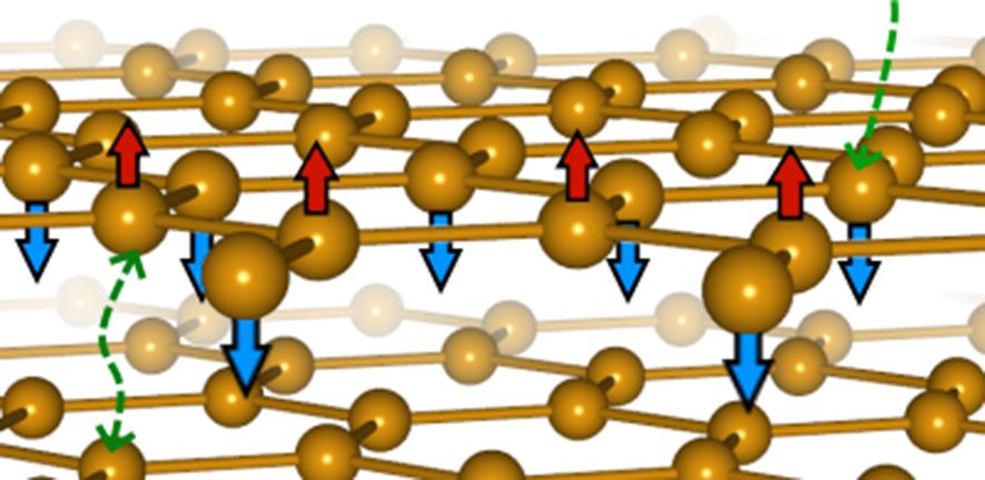
In what follows, it will help if you have already read my paper on Period 4, where I diagram many of
the transition metals, showing how the charge streams are created. That is where this diagram of
Copper came from. In superconductivity, we will be following the polar or axial channel (from bottom
to top) in the above diagram. This is what I call the through charge stream, because it concerns charge
that passes straight through from south to north without being channeled out the carousel level. The
carousel level is composed of the disks on the equator, which spin as a whole east/west in a circle (like
a carousel). Normally, they pull charge from the poles to the equator, where the bulk of it is re-emitted.
It is the spin of the nucleus which causes this main stream, with the greater angular momentum at the
equator causing the greater charge emission there. In most cases and with most elements, the main or
primary charge stream is from pole to equator.
But when we are looking at what we call electrical conduction, we are looking at the stream from south
pole to north. This stream is linear, directionalized, and coherent. If we align the poles of adjacent
nuclei, we create longer lines of conduction.
As you can probably see already, this explains the Meissner Effect in superconductivity, where interior
magnetic lines disappear. We have never been given a simple mechanical explanation for that, but my
diagram of Copper supplies it immediately. If this Copper nucleus begins superconducting, that simply
means that all photons being recycled are going from pole to pole. None are being recycled out the
equatorial or carousel level. As we know, the magnetic field lines are always orthogonal to the
electrical field lines. Well, the electrical fields lines go with the conduction. They run south to north
here. The magnetic field lines are then orthogonal to that and in a circle, by the old right hand rule.
Well, since we have no photons being emitted out the equator in this case, we have no magnetic field
being created. Both the electrical field and magnetic field are caused by the charge field, and the
charge field is just the recycled photons. Photons that are recycled from south to north in a line create
the electrical field, and photons that are recycled through the carousel level create the magnetic field.
So if all charge is channeled south to north as through charge, nothing is left to create the magnetic
field. It disappears. This disappearance is what we call the Meissner Effect.
This tells us how the magnetic field and electrical field are related at the foundational level. Given my
theory, we should have expected the magnetic field to go to zero when the electrical field was at a
maximum, since the field creation is a zero-sum game. Since the same charge field creates both, a
maximal electrical conduction implies a zero magnetic field. If all charge photons are being conducted,
none can be left to create the magnetic field (internally). Since all photons are spinning, the external
electrical field will still have a potential magnetic component, but in the atoms themselves, there is
nothing that we would call a magnetic field. Given superconduction, those internal field lines are gone.
Now, if we plug an Oxygen into that Copper nucleus, we can increase conduction even more, since the
Oxygen will plug in on the pole (see diagram below). Our recycling engine will be bigger, having
more fans to pull charge through (as it were). And the added fans will all be aligned on the pole,
increasing through charge. Under normal circumstances, CuO will still recycle some of the charge out
the carousel level, so we will not have superconduction. This begs the question: how can we cause
superconduction? What would we do to maximize conduction? Well, obviously we would minimize
charge recycling on the equator. That would force all recycling to happen on the pole. The easiest way
to do that is stop the carousel level from spinning. If the nucleus stops spinning about its axis, we no
longer have more angular momentum on the equator, and no reason for charge to recycle out that way.
This is what happens with supercold superconduction. But what happens with warmer
superconduction? To figure that out, we have to look at how it is created in the lab. We need to add
Mercury, Calcium and Barium to our diagram.
"
[/quote]
Keep in mind Purple:
---
more at link: https://gizmodo.com/this-2000-year-old-pigment-can-eliminate-the-third-dime-1661476168
Han purple is an ancient pigment that wasn't reconstructed by modern chemists until 1992. After the chemists got done with it, it was the physicists' turn. Han purple, they found, eliminates an entire dimension. It makes waves go two-dimensional!
The Chemistry of Han Purple
You'll see Han purple on the famous terracotta warriors surrounding the tomb of the first emperor of China, or on ancient pottery and other works of art. Where you won't see it is on anything made between 220 A.D. and 1992, because after the pigment disappeared it took 1700 years to re-discover it. Elisabeth FitzHugh, a conservator at the Smithsonian, pinned down the chemical composition of the pigment and announced it was a barium copper silicate. (The paper describing the discovery is a fun read. It starts by pointing out the inferiority of other ancient purple pigments, which tended to be closer to red than purple. It also stresses that Tyrian purple, made from sea snails, was a textile dye, not a pigment, and that it could range anywhere from "reddish-blue to purplish-violet." Take that, Phoenicians!)'
http://www.jstor.org/discover/10.2307/1506342?uid=2&uid=4&sid=21105259747793
A purple barium copper silicate, BaCuSi2O6 an artificial inorganic pigment, has been identified, sometimes mixed with the known blue barium copper silicate, BaCuSi4O10. It occurs on painted objects and in octagonal sticks from China attributed to the Han dynasty (208 BC-AD 220). This man-made pigment, for which the name Han purple is proposed, has not been previously characterized.


Wikipedia wrote:
Chemical formula
CuO25P6Pb9
Molar mass 2514.2 g·mol−1
Appearance Purple crystal when pure[1]
Density ≈6.699 g/cm3
Similar structured molecules in the Physics database:
Formula
BaCuOPb
BaCuOPt
CuOPb
H3BCuNa3O12PSZn
H8Cu3O9P2
NEWS
16 August 2023
LK-99 isn’t a superconductor — how science sleuths solved the mystery
Efforts to replicate the material have pieced together the puzzle of why it displayed superconducting-like behaviours.
Dan Garisto
Shards of a purple crystal on a table.
https://www.nature.com/articles/d41586-023-02585-7
related: https://www.nature.com/articles/d41586-023-02481-0
Pure crystals of LK-99, synthesized by a team at the Max Planck Institute for Solid State Research in Stuttgart, Germany. Credit: Pascal Puphal
Researchers seem to have solved the puzzle of LK-99. Scientific detective work has unearthed evidence that the material is not a superconductor, and clarified its actual properties.
The conclusion dashes hopes that LK-99 — a compound of copper, lead, phosphorus and oxygen — would prove to be the first superconductor that works at room temperature and ambient pressure. Instead, studies have shown that impurities in the material — in particular, copper sulfide — were responsible for sharp drops in its electrical resistivity and a display of partial levitation over a magnet, properties similar to those exhibited by superconductors.
“I think things are pretty decisively settled at this point,” says Inna Vishik, a condensed-matter experimentalist at the University of California, Davis.
Claimed superconductor LK-99 is an online sensation — but replication efforts fall short
The LK-99 saga began in late July, when a team led by Sukbae Lee and Ji-Hoon Kim at the Quantum Energy Research Centre, a start-up firm in Seoul, published preprints1,2 claiming that LK-99 is a superconductor at normal pressure, and at temperatures up to at least 127 ºC (400 kelvin). All previously confirmed superconductors function only at very low temperatures and extreme pressures.
The extraordinary claim quickly grabbed the attention of the science-interested public and researchers, some of whom tried to replicate LK-99. Initial attempts did not find signs of room-temperature superconductivity, but were not conclusive. Now, after dozens of replication efforts, many specialists are confidently saying that the evidence shows LK-99 is not a room-temperature superconductor. (Lee and Kim’s team did not respond to Nature’s request for comment.)
Accumulating evidence
The South Korean team based its claim on two of LK-99’s properties: levitation above a magnet and abrupt drops in resistivity. But separate teams at Peking University3 and the Chinese Academy of Sciences4 (CAS), both in Beijing, found mundane explanations for these phenomena.
Another study5, by researchers in the United States and Europe, combined experimental and theoretical evidence to demonstrate how LK-99’s structure made superconductivity infeasible. And other experimenters synthesized and studied pure samples6 of LK-99, erasing doubts about the material’s structure and confirming that it is not a superconductor, but an insulator.
The only further confirmation would come from the South Korean team sharing its samples, says Michael Fuhrer, a physicist at Monash University in Melbourne, Australia. “The burden’s on them to convince everybody else,” he says.
Perhaps the most striking evidence for LK-99’s superconductivity was a video taken by the South Korean team that showed a coin-shaped sample of silvery material wobbling over a magnet. The researchers said that the sample was levitating because of the Meissner effect — a hallmark of superconductivity in which a material expels magnetic fields. Multiple unverified videos of LK-99 levitating subsequently circulated on social media, but none of the researchers who initially tried to replicate the findings observed any levitation.
Half-baked levitation
Several red flags popped out to Derrick VanGennep, a former condensed-matter researcher at Harvard University in Cambridge, Massachusetts, who now works in finance but was intrigued by LK-99. In the video, one edge of the sample seemed to stick to the magnet, and it seemed delicately balanced. By contrast, superconductors that levitate over magnets can be spun and even held upside down. “None of those behaviours look like what we see in the LK-99 videos,” VanGennep says.
He thought LK-99’s properties were more likely to be the result of ferromagnetism. So he constructed a pellet of compressed graphite shavings with iron filings glued to it. A video made by VanGennep shows that his disc — made of non-superconducting, ferromagnetic materials — mimicked LK-99’s behaviour.
On 7 August, the Peking University team reported3 that this “half-levitation” appeared in its own LK-99 samples because of ferromagnetism. “It’s exactly like an iron-filing experiment,” says team member Yuan Li, a condensed-matter physicist. The pellet experiences a lifting force, but it’s not enough for it to levitate — only for it to balance on one end.
Li and his colleagues measured their sample’s resistivity, and found no sign of superconductivity. But they couldn’t explain the sharp resistivity drop seen by the South Korean team.
Impure samples
The South Korean authors noted one particular temperature at which LK-99 showed a tenfold drop in resistivity, from about 0.02 ohm-centimetres to 0.002 Ω cm. “They were very precise about it: 104.8 ºC,” says Prashant Jain, a chemist at the University of Illinois at Urbana–Champaign. “I was like, wait a minute, I know this temperature.”
The reaction that synthesizes LK-99 uses an unbalanced recipe. For every one part that it makes of copper-doped lead phosphate crystal — pure LK-99 — it produces 17 parts copper and 5 parts sulfur. These leftovers lead to numerous impurities — especially copper sulfide (Cu2S), which the South Korean team reported finding in its sample.
Jain, a copper-sulfide specialist, remembered 104 ºC as the temperature at which Cu2S undergoes a phase transition. Below that temperature, the resistivity of air-exposed Cu2S drops dramatically — a signal almost identical to LK-99’s purported superconducting phase transition. “I was almost in disbelief that they missed it,” says Jain, who published a preprint7 on the important confounding effect.
On 8 August, the CAS team reported4 on the effects of Cu2S impurities in LK-99. “Different contents of Cu2S can be synthesized using different processes,” says team member Jianlin Luo, a CAS physicist. The researchers tested two samples — the first heated in a vacuum, which resulted in 5% Cu2S content, and the second in air, which gave 70% Cu2S content.
The first sample’s resistivity increased smoothly as it cooled, as did samples from other replication attempts. But the second sample’s resistivity plunged near 112 ºC (385 K) — closely matching the South Korean team’s observations.
“That was the moment where I said, ‘Well, obviously, that’s what made them think this was a superconductor,’” says Fuhrer. “The nail in the coffin was this copper sulfide thing.”
Making conclusive statements about LK-99’s properties is difficult, because the material is unpredictable and samples contain varying impurities. “Even from our own growth, different batches will be slightly different,” says Li. But he argues that samples that are close enough to the original are sufficient for checking whether LK-99 is a superconductor in ambient conditions.
Crystal clear
With strong explanations for the resistivity drop and the half-levitation, many in the community were convinced that LK-99 was not a room-temperature superconductor. But mysteries lingered — namely, what were the material’s actual properties?
Initial theoretical attempts using an approach called density functional theory (DFT) to predict LK-99’s structure had hinted at interesting electronic signatures known as flat bands. These are areas where the electrons move slowly and can be strongly correlated. In some cases, this behaviour leads to superconductivity. But these calculations were based on unverified assumptions about LK-99’s structure.
To better understand the material, the US–European group5 performed precision X-ray imaging of its samples to calculate LK-99’s structure. Crucially, the imaging allowed the team to make rigorous calculations that clarified the situation of the flat bands, showing that they were not conducive to superconductivity. Instead, the flat bands in LK-99 came from strongly localized electrons, which cannot ‘hop’ in the way that a superconductor requires.
On 14 August, a separate team at the Max Planck Institute for Solid State Research in Stuttgart, Germany, reported6 synthesizing pure, single crystals of LK-99. Unlike previous synthesis attempts, which had relied on crucibles, this one used a technique called floating-zone crystal growth. This enabled the researchers to avoid introducing sulfur into the reaction, thereby eliminating the Cu2S impurities.
The result was a transparent purple crystal — pure LK-99, or Pb8.8Cu1.2P6O25. Separated from impurities, LK-99 is not a superconductor, but an insulator with a resistance in the millions of ohms — too high for a standard conductivity test to be run. It shows minor ferromagnetism and diamagnetism, but not enough for even partial levitation. “We therefore rule out the presence of superconductivity,” the team concluded.
The team suggests that the hints of superconductivity seen in LK-99 were caused by Cu2S impurities, which are absent from their crystal. “This story is exactly showing why we need single crystals,” says Pascal Puphal, a specialist in crystal growth and the Max Planck physicist who led the study. “When we have single crystals, we can clearly study the intrinsic properties of a system.”
Lessons learnt
Many researchers are reflecting on what they’ve learnt from the summer’s superconductivity sensation.
For Leslie Schoop, a solid-state chemist at Princeton University in New Jersey, who co-authored the flat-bands study, the lesson about premature calculations is clear. “Even before LK-99, I have been giving talks about how you need to be careful with DFT, and now I have the best story ever for my next summer school,” she says.
Jain points to the importance of old, often overlooked data — the crucial measurements that he relied on for the resistivity of Cu2S were published in 1951.
Although some commentators have pointed to the LK-99 saga as a model for reproducibility in science, others say that it involved an unusually swift resolution of a high-profile puzzle. “Often these things die this very slow death, where it’s just the rumours and nobody can reproduce it,” says Fuhrer.
When copper oxide superconductors were discovered in 1986, researchers leapt to probe their properties. But nearly four decades later, there is still debate over the materials’ superconducting mechanism, says Vishik. Efforts to explain LK-99 came readily. “The detective work that wraps up all of the pieces of the original observation — I think that’s really fantastic,” she says. “And it’s relatively rare.”
doi: https://doi.org/10.1038/d41586-023-02585-7
References
Lee, S. et al. Preprint at https://arxiv.org/abs/2307.12037 (2023).
Lee, S., Kim, J.-H. & Kwon, Y.-W. Preprint at https://arxiv.org/abs/2307.12008 (2023).
Guo, K., Li, Y. & Jia, S. Sci. China Phys. Mech. Astron. https://doi.org/10.1007/s11433-023-2201-9 (2023).
Article
Google Scholar
Zhu, S., Wu, W., Li, Z. & Luo, J. Preprint at https://arxiv.org/abs/2308.04353 (2023).
Jiang, Y. et al. Preprint at https://arxiv.org/abs/2308.05143 (2023).
Puphal, P. et al. Preprint at https://arxiv.org/abs/2308.06256 (2023).
Jain, P. K. Preprint at https://arxiv.org/abs/2308.05222 (2023).
Last edited by Chromium6 on Sun Aug 20, 2023 3:54 pm; edited 1 time in total
Chromium6- Posts : 727
Join date : 2019-11-29
Re: Mathis on Graphene? Any hints?
![]() by Chromium6 Sun Aug 20, 2023 1:25 am
by Chromium6 Sun Aug 20, 2023 1:25 am
--------
AgBaCeCuO
AgBaCuDyO
AgBaCuGdO
AgBaCuOSm
Al2CuO4
Al4Cu2O7
AlCuO2
B2Cu3O6
B2CuO4
Ba2CaCu2HgO6
Ba2Cu2Te4O11Br2
Ba2Cu3OY
Ba2CuBrO2
Ba2CuClO2
Ba2CuTeO6
Ba2TlCuHgO5
Ba2TlCuO5
Ba2YCu3O7
Ba2YCu3O8
Ba2YTlCu2O7
Ba3Y2Cu2PtO10
BaCuHoORh
BaCuMoO
BaCuO5Y2
BaCuOPb
BaCuOPt
BaSi2CuO6
BaSr2CaCu4O8
BaYFeCuO5
Bi2Sr2CaCu2O
Bi2Sr2CaCu2O8
Bi2Sr2TeCu3O8
BiPbSr2Ca2Cu3O10
BiSnBa4TmCaCu4O14
C2CuO4
Ca2CuO2Br2
Ca2CuO2Cl2
Ca2Eu2Cu2O6Cl2
Ca2FeCuSeO3
Ca2FeCuSO3
Ca2Gd2Cu2O6Cl2
Ca3Cu2O4Br2
Ca3Cu2O4Cl2
CaCu2O3
CaCuO2
CaSmCuO3Cl
CCuO3
Cd2CaCu3O6
Cd3CaCu4O8
CdCaCu2O4
CdNbBa9Cu10O20
CoCu2O3
CoCuO2
CoCuP2O7
Cr2Cu4O12
CrCu2O8F6
CrCuO
CrCuO2
CrCuO4
CsCu3O2
CsCuO
CsCuO2
Cu10C4O24
Cu2Ag2O3
Cu2As2O7
Cu2AsClO4
Cu2Cl2O
Cu2ClO3
Cu2GeO4
Cu2M9O3
Cu2Mo3Se4
Cu2N2S2O6
Cu2NSe2O10
Cu2O
Cu2O2
Cu2O3S
Cu2O4
Cu2O4F2
Cu2P2O7
Cu2Pb2S2O12
Cu2PbO2
Cu2Po
Cu2SO4
Cu2SO5
Cu2Te3O8
Cu3BiSe2O8
Cu3BiTe2O8Cl
Cu3C4P2S2O16
Cu3MgO4
Cu3O6S2
Cu3Pb2NSe2O11
Cu3PbTeO8
Cu3Se2O6Cl2
Cu3Te2O6Br2
Cu3Yb2Te4O12Cl4
Cu4As4O22
Cu4Cd2Te6O16Cl4
Cu4N2O12
Cu4O3
Cu4O4Cl4
Cu4O6
Cu4O6Cl2
Cu4SO10
Cu6PbO8
Cu8S2O24
Cu9Pb2Se4O16Cl4
CuAgO2
CuAsPbO4
CuB4O7
CuBiSeO
CuBiTeO
CuC2S2O6F6
CuCClO
CuCl3O2
CuCO
CuCO3
CuCOCl
CuGeO3
CuI2O6
CuMgMoS
CuMgO2
CuMoO4
CuN2O6
CuN3O9
CuNb2O6
CuO
CuO2
CuO3Si
CuO3Sn
CuO3Ti
CuO3Zr
CuO4W
CuO6I2
CuO8S2Zn
CuOPb
CuOSn
CuPb2O4Cl2
CuPb4S2O14
CuPo
CuSb2O3Cl
CuSb6S2O16
CuSe2O5
CuSeO3
CuSeO4
CuSiO3
CuSO4
CuTeO3
CuTeO4
CuWO3F2
CuWO4
FeCu2O8F6
FeCuC5N6O3
FeCuO2
Ga2Sr4Tm2CaCu5O2
Ga2Sr4Y2CaCu5O2
GaCuO2
H10CuNb2O6
H12B2CuF8O6
H14CuN4O5S
H16Ba2Ca2Cu3HgO8
H2B2CuF8O
H2Cr2CuO8
H2Cu3O10S2
H2Cu3O2
H2CuNb2O6
H2CuO5S
H3BCuNa3O12PSZn
H4Cl2CuO2
H4CuN2O7
H4CuO4Se
H4CuO5Se
H8Cu3O9P2
HgBaCaCuO
In4Sn2Ba2MnCu7O14
In4Sn2Ba2TiCu7O14
In5Ba4SiCu8O16
In5Sn2Ba2SiCu8O16
In6Sn2Ba2SiCu9O13
In7Sn2Ba2SiCu10O20
InCu6ClO8
InCuO2
K2Cu3Se4O12
K2CuP2O7
K2CuSO4Cl2
K2Mo2Cu2O10
K4Cu4O4
KCuCO3F
KCuO
KCuO2
KNa2CuO2
LaBaCa2Cu4O2
Li2Cu2TeO6
Li2V2Cu4O12
LiCuO
LiCuO2
LiCuO2H4Cl3
LiVCuO4
MgCu2O3
MgCu2TeO12
MgCu3O6H6Cl2
Mn2CuO4
MnCuO2
Na2Cu2TeO6
Na2Si4Cu2O11
Na3Cu2SbO6
Na4Cu4O4
Na5CuSO2
NaCuO
NaCuO2
NaCuSO4F
NbBa9Cu10O20
NbCuO3
NbCuO3F
Pb3Sn3Sr8Ca4Cu10O30
Pb3Sr4Ca3Cu6O2
PbGaSr4YCaCu4O2
Pr2CeCuO4
Rb3CuO2
RbCuO
RbCuO2
ScCuO2
SiCuO3
Sn10SbTe4Ba2MnCu16O32
Sn3Ba4Ca2Cu7O2
Sn3Ba4In3Cu6O2
Sn3Ba4Y2Cu5O2
Sn3BaBCa4Cu11O2
Sn3Sb3Ba2MnCu7O14
Sn4Ba41m2CaCu7O2
Sn4Ba4CaTmCu4O2
Sn4Ba4Tm3Cu7O2
Sn5InBa4Ca2Cu11O2
Sn5Sb5Ba2MnCu11O22
Sn6Ba4Ca2Cu10O2
Sn6Sb6Ba2MnCu13O26
Sn8SbTe4Ba2MnCu14O28
Sn9SbTe3Ba2MnCu14O28
Sn9SbTe4Ba2MnCu15O30
Sn9SbTe7Ba2MnCu17O34
Sn9SbTe8Ba2MnCu19O38
Sn9Te3Ba2MnCu13O26
Sr2Ca2Cu2Bi2O8
Sr2CaCu2Bi2O8
Sr2CrCuSO3
Sr2Cu2O3
Sr2Cu2O5
Sr2CuBi2O6
Sr2CuBrO2
Sr2CuClO2
Sr2CuO2Br2
Sr2CuO2Cl2
Sr2CuO2I2
Sr2FeCuSO3
Sr2GaCuSO3
Sr2MnCuSO3
Sr2Nd2Cu2O6Cl2
Sr2TlCuO5
Sr2YTlCu2O7
Sr3Fe2Cu2S2O5
Sr3Fe2Cu2Se2O5
Sr3Sc2Cu2S2O5
SrCu2O3
SrCuO2
SrCuO4H4
Ta2CuO6
TaBa9Cu10O20
TaCuO3
TeBa10Cu11O22
TeBa3Cu4O2
TeBa7Cu8O17
TeCaBa4Cu6O14
Ti2Ba2TeCu3O8
Ti2Ba2YCu2O6
Ti5Ba4Ca2Cu10O2
Ti5Ba4SiCu8O16
Ti5Pb2Ba2MgCu10O17
Ti5Pb2Ba2Si2.5Cu8.5O17
Ti5Pb2Ba2SiCu8O16
Ti5Sn2Ba2SiCu8O16
Ti6Ba4SiCu9O18
Ti7Sn2Ba2MnCu10O20
Ti7Sn2Ba2SiCu10O20
Ti7Sn2Ba2TiCu10O20
TiBa4TmCaCu5O2
TiBa7Cu8O16
TiBa9Cu10O20
TiSnBa4Y2Cu4O2
Tl2CuAsO4
TlCuHSeO5
TlCuHSO5
V2Cu2O7
V2CuN2O6H6
V4Cu2P4O28
VBa9Cu10O20
VCdCuO4
VCu3O4
VCuO3
W2Cu2O8
Y2Ba10Cu12O25
Y2BaSCu7O2
Y2BaSCu8O17
Y2CaBa4Cu7O16
Y2SnBa4Cu5O2
Y3Ba4Cu7O16
Y3Ba5Cu8O2
Y3CaBa4Cu8O18
YBa2Cu3O7
YCaBa3Cu5O11
YCu6ClO8
YCuO2
YSrCa2Cu4O8
ZrBa9Cu10O20
SELECT Distinct Formula
FROM [Physics].[dbo].[AtomicMilesMathisOrbitalsDetailAllBonds]
Where Formula like '%Cu%O%'
From what is loaded these 81 are superconductors in the literature:
Formula
BaSr2CaCu4O8
Bi2Sr2CaCu2O
Bi2Sr2CaCu2O8
Bi2Sr2TeCu3O8
BiPbSr2Ca2Cu3O10
BiSnBa4TmCaCu4O14
Cd2CaCu3O6
Cd3CaCu4O8
CdCaCu2O4
CdNbBa9Cu10O20
Cu2M9O3
Cu3MgO4
CuMgO2
Ga2Sr4Tm2CaCu5O2
Ga2Sr4Y2CaCu5O2
HgBaCaCuO
In4Sn2Ba2MnCu7O14
In4Sn2Ba2TiCu7O14
In5Ba4SiCu8O16
In5Sn2Ba2SiCu8O16
In6Sn2Ba2SiCu9O13
In7Sn2Ba2SiCu10O20
LaBaCa2Cu4O2
NbBa9Cu10O20
Pb3Sn3Sr8Ca4Cu10O30
Pb3Sr4Ca3Cu6O2
PbGaSr4YCaCu4O2
Pr2CeCuO4
Sn10SbTe4Ba2MnCu16O32
Sn3Ba4Ca2Cu7O2
Sn3Ba4In3Cu6O2
Sn3Ba4Y2Cu5O2
Sn3BaBCa4Cu11O2
Sn3Sb3Ba2MnCu7O14
Sn4Ba41m2CaCu7O2
Sn4Ba4CaTmCu4O2
Sn4Ba4Tm3Cu7O2
Sn5InBa4Ca2Cu11O2
Sn5Sb5Ba2MnCu11O22
Sn6Ba4Ca2Cu10O2
Sn6Sb6Ba2MnCu13O26
Sn8SbTe4Ba2MnCu14O28
Sn9SbTe3Ba2MnCu14O28
Sn9SbTe4Ba2MnCu15O30
Sn9SbTe7Ba2MnCu17O34
Sn9SbTe8Ba2MnCu19O38
Sn9Te3Ba2MnCu13O26
TaBa9Cu10O20
TeBa10Cu11O22
TeBa3Cu4O2
TeBa7Cu8O17
TeCaBa4Cu6O14
Ti2Ba2TeCu3O8
Ti2Ba2YCu2O6
Ti5Ba4Ca2Cu10O2
Ti5Ba4SiCu8O16
Ti5Pb2Ba2MgCu10O17
Ti5Pb2Ba2Si2.5Cu8.5O17
Ti5Pb2Ba2SiCu8O16
Ti5Sn2Ba2SiCu8O16
Ti6Ba4SiCu9O18
Ti7Sn2Ba2MnCu10O20
Ti7Sn2Ba2SiCu10O20
Ti7Sn2Ba2TiCu10O20
TiBa4TmCaCu5O2
TiBa7Cu8O16
TiBa9Cu10O20
TiSnBa4Y2Cu4O2
VBa9Cu10O20
Y2Ba10Cu12O25
Y2BaSCu7O2
Y2BaSCu8O17
Y2CaBa4Cu7O16
Y2SnBa4Cu5O2
Y3Ba4Cu7O16
Y3Ba5Cu8O2
Y3CaBa4Cu8O18
YBa2Cu3O7
YCaBa3Cu5O11
YSrCa2Cu4O8
ZrBa9Cu10O20
SELECT Distinct Formula, Cast(CAST(ZID AS DECIMAL(15,2) ) as nvarchar(20)) as T , ZID
FROM [Physics].[dbo].[AtomicMilesMathisOrbitalsDetailAllBonds]
Where Formula like '%Cu%O%'
) x
where RIGHT(Cast(CAST(ZID AS DECIMAL(15,2) ) as nvarchar(20)),3) = '.01'
Chromium6- Posts : 727
Join date : 2019-11-29
Re: Mathis on Graphene? Any hints?
![]() by Chromium6 Sat Sep 02, 2023 9:57 pm
by Chromium6 Sat Sep 02, 2023 9:57 pm
----------
Hopes fade for 'room temperature superconductor' LK-99, but quantum zero-resistance research continues
by Michael Fuhrer, The Conversation
The past few weeks have seen a huge surge of interest among scientists and the public in a material called LK-99 after it was claimed to be a superconductor at room temperature and ambient pressure.
LK-99 garnered attention after South Korean researchers posted two papers about it on arXiv, a non-peer-reviewed repository for scientific reports, on July 22. The researchers reported possible indicators of superconductivity in LK-99, including unexpectedly low electrical resistance and partial levitation in a magnetic field.
The potential discovery drew enthusiasm on social media and was widely reported in traditional media too. As a physicist working on quantum phenomena in materials, I was gratified to see the interest in superconductivity, and I shared in the excitement about the report. But I also approached the results with skepticism, especially since many previous reports of room-temperature superconductivity have failed to be reproduced.
Now, after follow-up experiments by scientists around the world, it seems LK-99 is not so special after all. However, while this particular avenue of research may be a dead end, the dream of a room-temperature superconductor is still very much alive.
What is a superconductor, and why are they useful?
You're probably familiar with ordinary conductors, like metals, in which electrons can move fairly easily through the "crystal lattice" of atoms that makes up the material. This means an electric current can flow—but the electrons are jostled around a bit as they move, so they lose energy as they travel. (This jostling is called electrical resistance.)
In a superconductor, there is zero resistance and an electrical current can flow perfectly smoothly without losing any energy. Many metals become superconductors at very low temperatures.
Superconductivity occurs when the electrons slightly distort the crystal lattice of the metal in a way that makes them team up into "Cooper pairs." These pairs of electrons then "condense" into a superfluid, a state of matter that can flow without friction.
Superconductors are very useful. They can be used to create extremely powerful electromagnets, such as those in MRI scanners, particle accelerators, fusion reactors and maglev trains.
Current superconductors work only at ultra-cold temperatures, so they require expensive refrigeration. A material that superconducts at everyday temperature and pressure could be used much more widely.
Currently, the highest superconducting temperatures at ambient pressure are around –138℃ (135 Kelvin), found in "cuprate" superconductors, a family of copper-containing compounds discovered unexpectedly in 1986. Electron pairing in the cuprates appears to involve a different mechanism than interaction with the lattice.
However, while our understanding of such exotic superconductors has improved, we still can't yet predict with any certainty new materials which could superconduct at even higher temperature. Still, there is no reason to think this can't be achieved. Moreover, many if not most superconducting materials are discovered serendipitously—so a claimed discovery of an unexpected room-temperature superconductor can't be dismissed out of hand.
So what about LK-99?
LK-99 is a compound containing oxygen, phosphorus, lead and copper. Little was known about the material when the papers claiming superconductivity emerged. For example, it wasn't even known whether it should conduct electricity at all.
The report of superconductivity at ambient conditions sparked a crash effort from researchers around the world to understand the material and reproduce the results. While it is still early days, and neither the initial report nor the follow-ups have been peer-reviewed, a picture has started to emerge that the LK-99 compound described by the authors is not a superconductor, and not even a metal.
So if it's not a superconductor, why did the original researchers think it was? One study has pointed out that an impurity in the initial LK-99 samples, cuprous sulfide, could explain some of what they saw.
Cuprous sulfide experiences a sudden, large change in resistance at a temperature of around 127℃ (400K). The first researchers saw this drop in resistance and attributed it to superconductivity in LK-99, but it is more likely explained by very low (not zero) resistance in the cuprous sulfide impurity.
The partial levitation of LK-99, which might have indicated a property of superconductors called "magnetic flux pinning," seems to be caused by ferromagnetism, a familiar effect that occurs in iron and many other materials.
So while nobody has proven the LK-99 samples studied in the original reports don't superconduct, the balance of evidence right now is strongly in favor of other explanations. Most scientists studying superconductivity don't see much reason to continue looking at LK-99.
Excitons and beyond
What's next for superconductivity research? Well, we can cross LK-99 off the list of materials to study, but the search goes on.
In fact, there has been a lot of progress in the past few years towards creating zero resistance under ordinary conditions.
Making electrons pair together is the key to superconductivity, but this is hard to do as they naturally repel each other. However, it's possible to make an electron pair up with a "hole" in a material—a gap where an electron should be.
These electron–hole pairs are called excitons, and they can be combined with light to form a frictionless superfluid at room temperature. This superfluid doesn't carry an electrical current (because the charges of the electron and the hole cancel out), but separating the electron and hole might allow supercurrents without resistance.
Topological insulators
An alternate route to zero resistance at room temperature has been found in so-called topological insulators. These are materials that only allow electrons to move along their edges or surfaces, in some cases with no resistance.
Graphene, a material made of sheets of carbon only a single atom thick, can be turned into a topological insulator in a strong magnetic field. But the required magnetic field is so extreme it can only be realized in a few laboratories in the world.
There are also other types of topological insulators that work without an externally applied magnetic field. Current versions of these materials show zero resistance only at very low temperatures, but there appears to be no reason they couldn't work at room temperature.
More at link: https://phys.org/news/2023-08-room-temperature-superconductor-lk-quantum.html
Youtube vids:
Agustin Schiffrin discusses Superconductors:
https://www.youtube.com/watch?v=yLOemDX8lJg
Superconductor Breakthroughs: Why Investors...
https://www.youtube.com/watch?v=ZihQyeVUMKs
Magnetic Flux Pinning:
https://www.youtube.com/watch?v=OSojjjvRCR0
Chromium6- Posts : 727
Join date : 2019-11-29
Re: Mathis on Graphene? Any hints?
![]() by Chromium6 Sat Sep 02, 2023 10:06 pm
by Chromium6 Sat Sep 02, 2023 10:06 pm
Miles' on the Meissner Effect:
http://milesmathis.com/conduct.html
http://milesmathis.com/limat.pdf
http://milesmathis.com/solidlight.pdf
http://milesmathis.com/sl2.pdf
---------
Flux Pinning
Introduction
Flux pinning is a phenomenon that occurs when magnetic flux eddies in a type II superconductor are prevented from moving within the bulk of the superconductor, causing magnetic field lines to be 'pinned' in their positions. The superconductor must be a type II superconductor, because a type I superconductor cannot penetrate a magnetic field. Some type I superconductors can suffer from flux pinning if they are thin enough. A magnetic field can pass through a material if its thickness is comparable to the London penetration depth. The penetrating action of magnetism enables the fixation of the magnetic flux. At higher magnetic fields (above Hc1 and below Hc2), superconductors allow magnetic flux to enter quantized packets surrounded by superconducting current vortices (see Quantum vortices). These penetration sites are known as flux tubes. The number of flux tubes per unit area is proportional to the magnetic field with a proportionality constant equal to the flux quantum. On a simple disk 76 mm in diameter and 1 micron thick, next to a magnetic field of 28 kA/m, there are about 100 billion flux tubes that hold 70,000 times the weight of a superconductor. At low temperatures the flux tube is fixed in place and cannot move. This pinning holds the superconductor in place, thereby allowing it to float. This phenomenon is closely related to the Meissner effect, but with one crucial difference. The Meissner effect shields the superconductor from all magnetic fields that cause repulsion, unlike the fixed state of the superconductor disk, which holds the magnetic flux and the superconductor in place.
https://academic-accelerator.com/encyclopedia/flux-pinning
MEISSNER OR FLUX PINNING?
Jul 24, 2022
Qualitative Experiment steps:
Quantum Levitation is the stable levitation and suspension of a superconductor in a surrounding magnetic field. It is actually the result of two separate phenomena:
Meissner effect – the repulsion of magnetic fields from the superconductor body
Flux pinning – the pinning of magnetic flux inside the superconductor
We can perform the following experiments to distinguish between the two –
Meissner effect:
Take a Quantum Levitator and place it upside down, with the superconductor at the bottom facing up.
Cool with liquid nitrogen. Make sure not to over fill the nitrogen liquid.
Take a small magnet (like this) and gently drop it a few inches/cm above the superconductor.
It will jump right up, being repelled from the superconductor. This is perfect diamagnetism caused by the Meissner effect.
Flux pinning:
Repeat the same setup with the levitator upside down and cooled.
This time, push the magnet using plastic tweezers closer to the superconductor. Make sure to push the magnet close enough to feel the resistance.
Now, when you release the magnet – it stays floating, rotating around its symmetry axis.
https://quantumlevitation.com/meissner-or-flux-pinning/
--
Wikipedia:
https://en.wikipedia.org/wiki/Flux_pinning
https://en.wikipedia.org/wiki/Meissner_effect
Chromium6- Posts : 727
Join date : 2019-11-29
Re: Mathis on Graphene? Any hints?
![]() by Chromium6 Sat Sep 16, 2023 2:29 am
by Chromium6 Sat Sep 16, 2023 2:29 am
Jhantu Kumar Sahacorresponding author and Animesh Dutta
Author information Article notes Copyright and License information PMC Disclaimer
Abstract
Single-atom-thick graphene is a particularly interesting material in basic research and applications owing to its remarkable electronic, mechanical, chemical, thermal, and optical properties. This leads to its potential use in a multitude of applications for improved energy storage (capacitors, batteries, and fuel cells), energy generation, biomedical, sensors or even as an advanced membrane material for separations. This paper provided an overview of research in graphene, in the area of synthesis from various sources specially from biomass, advanced characterization techniques, properties, and application. Finally, some challenges and future perspectives of graphene are also discussed.
Graphic Abstract
An external file that holds a picture, illustration, etc.
Object name is 12649_2021_1577_Figa_HTML.jpg
Keywords: Graphene, Energy generation, Solar cells, Energy storage, Capacitors, Batteries, Fuel cells, Biomedical, Sensors, Membrane, COVID-19
Statement of Novelty
Reduction from graphene oxide is one of the most promising ways and is probably the most widely accepted method in graphene synthesis. Unfortunately, very few commercial technologies involving graphene-based materials have emerged, in large part due to the difficulty in processing these 2D sheets into useful, 3D materials with predicable structure and thus function. Our proposed novel graphene synthesis from biomass sources will provide an alternative, inexpensive, and more versatile approach to make large area graphene. The application of our graphene from biomass sources and with many polymer composites will lead to the revolution in many sectors including biomedical, energy sectors. Continued development and successful implementation of graphene from biomass sources that could lead to new jobs and a potentially huge source of revenue to fuel the future economy.
Introduction
Single-atom-thick graphene is a particularly interesting material in basic research and applications owing to its remarkable electronic, mechanical, chemical, thermal, and optical properties [1]. For a given surface area, it is the lightest weight electronic conductor of any material and can be produced relatively inexpensively, and in large volume, from natural graphite resource. This leads to its potential use in a multitude of applications for improved energy storage (capacitors, batteries, and fuel cells), energy generation (solar cells), biomedical, sensors or even as an advanced membrane material for separations.
A lot of effort had been devoted for creating high-quality large-area graphene. The earliest method, mechanical exfoliation of graphene from highly oriented pyrolytic graphite using scotch tape, yields good quality but μm-sized graphene [2]. In addition, it is uncontrollable and not scalable. Other formation techniques, such as epitaxial graphene from a single crystalline SiC substrate [3–8] or transition metals [9–14], can yield larger graphene domains. However, they encounter difficulty for large-scale production due to the high cost of the substrates, the requirement of ultrahigh vacuum, and limited scalability. Recently, high-quality monolayer or bilayer graphene was obtained via the chemical vapor deposition (CVD) of CH4 or C2H2 gases on copper or nickel substrates [15–20]. Commercial wafer-scale and 30-in. (76.2 cm) graphene films have been reported [20, 21]. Currently, CVD technique is widely employed and has great potential for the large-scale production of high quality films [22–29]. However, since the CVD growth of high quality graphene requires a nearly oxygen-free environment or high-vacuum (10−6 Torr) base pressure, a long pumping and/or purge time is needed to evacuate the air in the chamber [30–35]. In addition, some of the gaseous raw materials are hazardous. These disadvantages limit its use in some applications and are a concern for large-scale production. Recently, much simpler, less expensive, and less hazardous techniques for growing graphene have been demonstrated [36–42]. These techniques use solid carbon sources (e.g., polymers, SiC, and amorphous carbon). For a Ni catalyst, carbon atoms diffuse into the Ni film during a high-temperature annealing process. Some of the C atoms segregate from the bulk to the Ni surface due to lower solid solubility at lower temperature [43]. A graphene layer forms with a specific and well-controlled cooling rate in a high-vacuum environment [44, 45]. A nearly oxygen-free environment is required in the graphene growth process not only to prevent the precipitated carbon from reacting with oxygen but also to avoid catalyst surface oxidation at high temperature. If graphene can be grown in a non-vacuum environment could open new applications. Many recent works [29, 37, 46] have shown that graphene can be grown at the interface of silicon dioxide and metal catalysts and Pt-based catalyst approach is also useful and was discussed in reference [47]. Moreover, a very important catalyst-free approach was also presented in reference [48]. Presently, there are several synthesis routes of graphene such as mechanical, chemical exfoliation, chemical vapor deposition, pyrolysis, epitaxial methods for obtaining graphene films [49]. A scheme depicting various conventional synthesis methods of graphene along with their important features, and their current and prospective applications are discussed in reference [50].
Unfortunately, very few commercial technologies involving graphene-based materials have emerged, in large part due to the difficulty in processing these 2D sheets into useful, 3D materials with predicable structure and thus function. To address this challenge, this research aims to develop new sources, tools, and processes to create a platform of graphene-based materials whose structure can be manipulated and fine-tuned at the nanoscale. Among these methods, reduction from graphene oxide is one of the most promising ways and is probably the most widely accepted method in large scale preparation. Considering both the scalability of this method and the purity of the final product, reduction of graphene oxide is better than other techniques. Nevertheless, industrialization with low cost is one of the major challenges in graphene field. With such consideration, the mechanical exfoliation and reduction of graphene oxide are the two possible methods for bulk production of graphene. On the other hand, pyrolysis and other chemical etching and gasification have been common techniques to synthesize graphene on metal surfaces from different carbon sources or other activated carbons [36, 51–57]. These also can be achieved by developing processes capable of depositing large-area monolayer graphene films onto a variety of substrates from biomass sources. However, the preparation of graphene by surface growth is limited in yield.
To develop devices based on graphene based materials from various sources, several synthetic schemes for the preparation of graphene including 3D graphene-based materials, and their properties, advanced characterization techniques, properties and their application for energy generation and storage, sensing, biomedical areas. Finally, analysis and challenges along with their future perspectives have been reviewed in discussion section:
Go to:
Materials and Methods
This section firstly presents an overview various synthesis technique that is used for the development of graphene from various sources including graphite, non-graphite sources followed by graphene synthesis from bio-mass sources.
Synthesis from Graphite Sources
Micromechanical Cleavage-the Scotch Tape Method Graphene can be extracted from the high-quality of graphite using mechanical exfoliation, which is a simple peeling process. Mechanical exfoliation of graphite using scotch tape is obtained from a commercially available highly oriented pyrolytic graphite (HOPG) sheet by dry etching in oxygen plasma. These thin flakes are composed of monolayer or a few layers of graphene [58]. Optical microscope image of multilayer graphene using Micromechanical cleavage-the scotch tape method as shown in Fig. 1.
An external file that holds a picture, illustration, etc.
Object name is 12649_2021_1577_Fig1_HTML.jpg
Fig. 1
a Optical microscope image of multilayer graphene cleaved from bulk graphite using the “scotch tape method”. b AFM image of an edge of the flake. c AFM image of few-layer graphene. d SEM of a device used by Geim and Novoselov for their studies of the electric field effect in graphene. e Schematic of device in d. (Reprinted with permission from Ref. [1, 2])
Chemical Cleavage and Exfoliation The two-step process to obtain graphene from graphite oxide requires first exfoliating the bulk material and then reducing the individual sheets back to graphene as shown in Fig. 2. Exfoliation is usually achieved by sonicating graphite oxide in water, followed by centrifugation. The supernatant from this procedure is colloidal and contains few- and single-layer sheets of graphene oxide. This liquid can be left as is or drop-cast onto a substrate for further processing.
An external file that holds a picture, illustration, etc.
Object name is 12649_2021_1577_Fig2_HTML.jpg
Fig. 2
Spin-coating technique employed in the deposition of graphene oxide on a surface. b AFM image of thin film spin-coated graphene oxide. c Optical microscope image of the delamination of rGO film from its substrate. d Floating rGO film ready for transfer onto an arbitrary substrate. (Reprinted with permission from Refs. [59, 60])
Synthesis from Non-graphitic Sources
Epitaxial Growth from Silicon Carbide Among the many graphene synthesis methods, the epitaxial growth approach from silicon carbide could help large-size and single-domain graphene production in a controlled manner. Supporting substrate is very important to access the intrinsic electronic properties of graphene. This lack of suitable substrate has so far been a major hurdle for the epitaxial growth of graphene using PECVD [61].
Physical Vapor Deposition Multiplayer graphene carbon films can be produced using simplified filtered cathodic vacuum arc (FCVA) deposition system. Carbon films were deposited using a FCVA system equipped with a double bend magnetic filter to minimize the deposition of macroparticles [61]. These macroparticle can be ejected from the carbon cathode as shown in Fig. 3.
An external file that holds a picture, illustration, etc.
Object name is 12649_2021_1577_Fig3_HTML.jpg
Fig. 3
Schematic diagram (not to scale) of the Filtered Cathode Vacuum Arc (FCVA) coating technology system. (Reprinted with permission from Ref. [62])
The schematic in Fig. 4 shows the steps involved in synthesis of the carbon films.
An external file that holds a picture, illustration, etc.
Object name is 12649_2021_1577_Fig4_HTML.jpg
Fig. 4
Schematic showing the growth sequence and transfer process employed to fabricate carbon films on silicon/silica substrates (Reprinted with permission from Ref. [63])
Chemical Vapor Deposition from CH4 Graphene single crystals can be grown using low-pressure chemical vapor deposition in copper-foil enclosures using methane as a precursor. The dimensions of graphene crystal could be up to 0.5 mm on a side (Fig. (Fig.55).
An external file that holds a picture, illustration, etc.
Object name is 12649_2021_1577_Fig5_HTML.jpg
Fig. 5
a Copper foil enclosure prior to insertion in the furnace. b Schematic of the CVD system for graphene on copper (Reprinted with permission from Ref. [19])
The CVD growth of graphene occurs on Cu grows by a surface adsorption process whereas the CVD growth of graphene on Ni occurs by a C segregation or precipitation process [64].
Conversion of Carbon Dioxide to Graphene The methodology produces few-layer graphene captured directly from CO2 by burning Mg in it. The combustion of magnesium metal in carbon dioxide to form few-layer graphene is unprecedented and provides further incentives for exploration of several environmentally friendly ways for capturing carbon dioxide [36, 65]. The burning magnesium metal in a CO2 environment produces carbon materials as shown in Eq. (1).
Growth of Graphene from Solid Carbon Sources Chemical Vapor Deposition (CVD) technique is limited to the use of gaseous raw materials, making it difficult to apply the technology to a wider variety of potential feedstocks. The large area, high quality graphene with controllable thickness can be grown from different solid carbon sources[ poly(methyl methacrylate) (PMMA), high impact polystyrene (HIPS), or acrylonitrile butadiene-styrene (ABS)] —such as polymer films or small molecules—deposited on a metal catalyst substrate at temperatures as low as 800 °C. Both pristine graphene and doped graphene were grown with this one-step process using the same experimental set-up [36].
Figure 6 illustrates the procedure for the growth of bilayer graphene directly on the SiO2 substrate. The SiO2 substrate was cleaned with oxygen-plasma and Piranha solution (4:1 sulfuric acid/hydrogen peroxide), and then a 400 nm thick nickel film was thermally evaporated onto the top of the SiO2 substrate used as the metal catalyst. Either solid polymers (PMMA, HIPS, or ABS) or gas-phase methane was used as a carbon source for the transfer-free growth of bilayer graphene.
An external file that holds a picture, illustration, etc.
Object name is 12649_2021_1577_Fig6_HTML.jpg
Fig. 6
Schematics of the growth of bilayer graphene from a solid carbon source. A 400 nm nickel film was thermally evaporated onto SiO2 substrate, followed by the spin-coating of polymers on the nickel. After annealing samples at 100 °C under a reductive Ar/H2 pressure for ∼ 10 min and then etching away the nickel, bilayer graphene is obtained directly on SiO2. The polymer film formation can be replaced by exposure to methane during the annealing step (Reprinted with permission from Ref. [66])
The two mechanisms of graphene growth on Ni and Cu can be understood from the C-metal binary phase diagram. The binary phase diagrams of C-Ni and C-Cu are similar in that C has a limited solubility in the metal without the presence of a metal-carbide line compound. The only significant difference is that the solubility of C in Cu is much lower than that in Ni. Since only a small amount of carbon can be dissolved in Cu, the source for graphene formation is mainly from the CH4 that is catalytically decomposed on the Cu surface with minimal carbon diffusion into the Cu. Once the surface is fully covered with graphene growth terminates because of the absence of a catalyst to decompose CH4 [19, 36, 63–66]
In contrast, Ni can dissolve more carbon atoms and hence it is difficult to get uniform graphene films due to precipitation of extra C during the cool-down. The C precipitation process is a nonequilibrium process, which should be suppressed if one aims to achieve monolayer graphene growth, for example, by using a controlled thin Ni film and/or high cooling rate. However, because of microstructural defects, predominantly grain boundaries, it is very difficult to fully eliminate the effect of precipitation for metals with high carbon solubility. Hence, metals with low C solubility such as Cu offer a possible path to large-area growth of graphene. Discrete regions of isotopically labelled graphene for growth on Cu may also yield novel devices and transport physics in future studies [19, 36, 63–66, 77–80]).
Moreover, a carbon diffusion mechanism through Ni layer is proposed for the growth mechanism of bilayer graphene on SiO2 substrates [66].
Graphene Ssynthesis from Polymers Graphene films can be formed directly on a SiO2/Si substrate from solution-processed common polymers. Patterned graphene layers can also be directly formed on active electronic devices without any physical transfer process as shown Fig. 7. The metal capping layer is used to prevent of vaporization of dissociated molecules and catalysis of graphene formation.
An external file that holds a picture, illustration, etc.
Object name is 12649_2021_1577_Fig7_HTML.jpg
Fig. 7
a Graphene growth process and b chemical structure of polymers used as graphene precursors (
reproduced with permission from Ref [67].)
Facile Synthesis of Graphene from Plastic by Pyrolysis of Poly(methyl ethacrylate), PMMA Figure 8 illustrates the preparation procedures of graphene by pyrolyzing PMMA composite. When the composite is heated at1000°C, PMMA is immediately decomposed into various carbon derivatives (Cn).
An external file that holds a picture, illustration, etc.
Object name is 12649_2021_1577_Fig8_HTML.jpg
Fig. 8
Illustration of the procedure for growth of the graphene on nickel particles by pyrolysis of PMMA composite: PMMA/OMT/Ni composite; (2) pyrolytic state in a specific microzone; (3) microstructure of hexagonal rings on Ni surface (4) continuous growth of graphene on Ni surface; (5) the graphene hybrid containing clay and catalyst; and (6) final purified graphene (Reprinted with permission from Ref. [68])
Based on the reported works, a summary and comparison of these preparation methods were listed in Table Table1.1. Some of the groundbreaking efforts in synthesizing graphene are summarized for graphene production in Ref. [69]. Among these methods, mechanical exfoliation and CVD can produce good-quality graphene. However, the practical application of graphene is blocked by the high price and insufficient supply.
more at link: https://www.ncbi.nlm.nih.gov/pmc/articles/PMC8446731/
Chromium6- Posts : 727
Join date : 2019-11-29
Re: Mathis on Graphene? Any hints?
![]() by Chromium6 Fri Oct 13, 2023 2:42 am
by Chromium6 Fri Oct 13, 2023 2:42 am
Unexpected Findings – Graphene Grows, and We Can See It
New York University
Popular University Of Amsterdam
By UNIVERSITY OF AMSTERDAM MAY 27, 2023
Graphene is a revolutionary material consisting of a single layer of carbon atoms arranged in a hexagonal lattice, offering incredible strength, conductivity, and flexibility. Its unique properties make it a promising candidate for various applications, from electronics and energy storage to medicine and environmental solutions.
Using ‘patchy particles’ as a model for graphene’s atomic structure, researchers have gained novel insights into the formation and evolution of defects in two-dimensional materials. This groundbreaking study uncovers the early formation and subsequent repair of the most common defect, which has important implications for future engineering and application of these materials.
Graphene stands unrivaled in terms of strength among all known materials. In addition to its unparalleled robustness, its superior conductivity of heat and electricity makes it an incredibly versatile and unique material. The unprecedented properties of graphene were so remarkable that its discovery was honored with the Nobel Prize in Physics in 2010. However, our comprehension of this material and its related substances remains largely incomplete, primarily due to the immense challenge in observing the atoms that constitute them. To overcome this obstacle, a collaborative research effort from the University of Amsterdam and New York University has discovered an unexpected solution.
Materials that exist in two dimensions, composed of an ultra-thin, singular layer of atomic crystals, have been receiving considerable interest in recent times. This heightened interest is largely attributed to their atypical attributes, which significantly differ from their three-dimensional ‘bulk’ counterparts.
Graphene, the most famous representative, and many other two-dimensional materials, are nowadays researched intensely in the laboratory. Perhaps surprisingly, crucial to the special properties of these materials are defects, locations where the crystal structure is not perfect. There, the ordered arrangement of the layer of atoms is disturbed and the coordination of atoms changes locally.
Visualizing atoms
Despite the fact that defects have been shown to be crucial for a material’s properties, and they are almost always either present or added on purpose, not much is known about how they form and how they evolve in time. The reason for this is simple: atoms are just too small and move too fast to directly follow them.
In an effort to make the defects in graphene-like materials observable, the team of researchers, from the UvA-Institute of Physics and New York University, found a way to build micrometer-size models of atomic graphene. To achieve this, they used so-called ‘patchy particles’.
Pieces of a Graphene Lattice Made From Patchy Particles
Pieces of a graphene lattice made from patchy particles. Because the particles can be followed one-by-one, defects can be studied at the particle scale. Credit: Swinkels et al.
These particles – large enough to be easily visible in a microscope, yet small enough to reproduce many of the properties of actual atoms – interact with the same coordination as atoms in graphene, and form the same structure. The researchers built a model system and used it to obtain insight into defects, their formation, and evolution with time. Their results were recently published in the scientific journal Nature Communications.
Building graphene
Graphene is made up of carbon atoms that each have three neighbors, arranged in the well-known ‘honeycomb’ structure. It is this special structure that lends graphene its unique mechanical and electronic properties. To achieve the same structure in their model, the researchers used tiny particles made of polystyrene, decorated with three even tinier patches of a material known as 3-(trimethoxysilyl)propyl – or TPM for short.
The configuration of the TPM patches mimicked the coordination of carbon atoms in the graphene lattice. The researchers then made the patches attractive so that the particles could form bonds with each other, again in analogy with the carbon atoms in graphene.
After being left alone for a few hours, when observed under a microscope the ‘mock carbon’ particles turned out to indeed arrange themselves into a honeycomb lattice. The researchers then looked in more detail at defects in the model graphene lattice. They observed that also in this respect the model worked: it showed characteristic defect motifs that are also known from atomic graphene. Contrary to real graphene, the direct observation and long formation time of the model now allowed the physicists to follow these defects from the very start of their formation, up to the integration into the lattice.
Unexpected results
The new look at the growth of graphene-like materials immediately led to new knowledge about these two-dimensional structures. Unexpectedly, the researchers found that the most common type of defect already forms in the very initial stages of growth, when the lattice is not yet established. They also observed how the lattice mismatch is then ‘repaired’ by another defect, leading to a stable defect configuration, which either remains or only very slowly heals further to a more perfect lattice.
Thus, the model system not only allows to rebuild the graphene lattice on a larger scale for all sorts of applications, but the direct observations also allow insights into atomic dynamics in this class of materials. As defects are central to the properties of all atomically thin materials, these direct observations in model systems help further engineer the atomic counterparts, for example for applications in ultra-lightweight materials and optical and electronic devices.
Reference: “Visualizing defect dynamics by assembling the colloidal graphene lattice” by Piet J. M. Swinkels, Zhe Gong, Stefano Sacanna, Eva G. Noya and Peter Schall, 18 March 2023, Nature Communications
.
DOI: 10.1038/s41467-023-37222-4
https://www.nature.com/articles/s41467-023-37222-4
Abstract
Graphene has been under intense scientific interest because of its remarkable optical, mechanical and electronic properties. Its honeycomb structure makes it an archetypical two-dimensional material exhibiting a photonic and phononic band gap with topologically protected states. Here, we assemble colloidal graphene, the analogue of atomic graphene using pseudo-trivalent patchy particles, allowing particle-scale insight into crystal growth and defect dynamics. We directly observe the formation and healing of common defects, like grain boundaries and vacancies using confocal microscopy. We identify a pentagonal defect motif that is kinetically favoured in the early stages of growth, and acts as seed for more extended defects in the later stages. We determine the conformational energy of the crystal from the bond saturation and bond angle distortions, and follow its evolution through the energy landscape upon defect rearrangement and healing. These direct observations reveal that the origins of the most common defects lie in the early stages of graphene assembly, where pentagons are kinetically favoured over the equilibrium hexagons of the honeycomb lattice, subsequently stabilized during further growth. Our results open the door to the assembly of complex 2D colloidal materials and investigation of their dynamical, mechanical and optical properties.
Introduction
Two-dimensional materials have attracted intense scientific interest, both from an application and a fundamental point of view, offering applications from light-weight materials to optoelectronic devices. These materials combine extraordinary mechanical, optical and electronic properties compared to bulk materials1,2,3. The most prominent representative, graphene, consists of a monolayer of carbon atoms bonded in a honeycomb lattice. The strong covalent bonds within the honeycomb lattice make the material particularly strong and light, while the honeycomb structure gives rise to a photonic and phononic band gap4,5. On a larger length scale, micrometre-size particles assembled into colloidal graphene, the analogue of atomic graphene assembled from colloidal particles, would open the door to two-dimensional multifunctional materials with photonic and phononic band gap for applications as 2D photonic and phononic crystals. However, producing large defect-free single-crystalline graphene of both atoms and colloids remains a great challenge, crucially limiting its applications.
Structural defects are known to be central to all of graphene’s properties, enabling among others band-gap tuning in graphene-based electronic devices6. However, while defects are introduced unavoidably during growth or added on purpose to tune mechanical and electronic properties, a comprehensive understanding of their formation is missing: because the trivalent carbon atoms or particles can arrange into a variety of polygons and structures, a coherent lattice exists even with defects, and rearrangements can take many paths. Despite advances in direct visualization of graphene defects using electron microscopy6,7,8, defect kinetics and healing remain poorly understood, and defect-free graphene challenging to produce.
Although colloidal particles are several orders of magnitude larger than atoms, their phase behaviour and dynamics are governed by the same thermodynamics principles. Phase behaviour of both atoms and colloids is largely governed by thermal forces, which means we can use colloidal aggregation and crystallization as a simple model for atomic crystallization9,10,11. One advantage of colloidal systems is that defect formation12,13,14 and dynamics15,16 can be conveniently studied directly in real time with single particle resolution using optical microscopy17,18, which remains challenging in atomic systems, especially under the harsh high-temperature atomic deposition used for graphene growth19. The recently-gained ability to synthesize anisotropic particles20,21,22,23, in particular colloidal particles with attractive patches providing specific valency and bond angles, has opened a design space for assembling more complex structures such as molecule analogues24,25,26 and covalently bonded crystals27,28.
Simulations and experiment have shown that these colloidal molecules can grow into larger assemblies, yielding rich structures ranging from the kagome lattice to buckyball-like clusters27,29. Experimentally realizing these structures remains challenging, as they require fine control over specifically coordinated interactions, or purposeful geometric design to block kinetically favoured nonequilibrium routes, as recently shown for the realization of colloidal diamond30,31. In contrast to tetrahedrally coordinated diamond, graphene relies on the trivalent coordination of particles. Patchy particles with patches at 120∘ angles can mimic these covalent bonds; yet, achieving such valency and controlling these directed bonds on the scale of kBT, the thermal energy, remains challenging, but would open up the assembly of structurally complex 2D materials, and investigation of their structural and mechanical properties.
Here, we assemble colloidal graphene and elucidate the kinetic pathways of crystallization and defect formation of this 2D material. We form the graphene lattice using pseudo-trivalent patchy particles adsorbed at a substrate, and directly follow the crystallization, defect formation and healing with great temporal and spatial resolution using confocal microscopy. Fine control of the patch-patch bond strength allows observation of near-equilibrium assembly in analogy to high-temperature deposition of atomic graphene. From the number of saturated bonds and the bond strain, we determine the configurational energy of the lattice and follow its evolution during lattice rearrangement and healing. Our results reveal that the most prominent defect motif of colloidal and atomic graphene, a pentagon, is kinetically favoured in the early stages of graphene growth, and acts as seed for extended defects during subsequent growth. These results hint at the importance of the early stages of assembly in generating defect-free graphene.
Chromium6- Posts : 727
Join date : 2019-11-29
Re: Mathis on Graphene? Any hints?
![]() by Chromium6 Mon Dec 18, 2023 1:09 am
by Chromium6 Mon Dec 18, 2023 1:09 am
Researchers have finally solved the long-standing puzzle of why graphene is so much more permeable to protons than expected by theory
Date: August 23, 2023
Source: University of Warwick
Summary:
Researchers have finally solved the long-standing puzzle of why graphene is so much more permeable to protons than expected by theory.
Researchers from The University of Warwick and the University of Manchester have finally solved the long-standing puzzle of why graphene is so much more permeable to protons than expected by theory.
A decade ago, scientists at The University of Manchester demonstrated that graphene is permeable to protons, nuclei of hydrogen atoms.
The unexpected result started a debate in the community because theory predicted that it would take billions of years for a proton to permeate through graphene's dense crystalline structure. This had led to suggestions that protons permeate not through the crystal lattice itself, but through the pinholes in its structure.
Now, writing in Nature, a collaboration between the University of Warwick, led by Prof. Patrick Unwin, and The University of Manchester, led by Dr. Marcelo Lozada-Hidalgo and Prof. Andre Geim, report ultra-high spatial resolution measurements of proton transport through graphene and prove that perfect graphene crystals are permeable to protons. Unexpectedly, protons are strongly accelerated around nanoscale wrinkles and ripples in the crystal.
The discovery has the potential to accelerate the hydrogen economy. Expensive catalysts and membranes, sometimes with significant environmental footprint, currently used to generate and utilise hydrogen could be replaced with more sustainable 2D crystals, reducing carbon emissions, and contributing to Net Zero through the generation of green hydrogen.
The team used a technique known as scanning electrochemical cell microscopy (SECCM) to measure minute proton currents collected from nanometre-sized areas. This allowed the researchers to visualise the spatial distribution of proton currents through graphene membranes.
If proton transport took place through holes as some scientists speculated, the currents would be concentrated in a few isolated spots. No such isolated spots were found, which ruled out the presence of holes in the graphene membranes.
Drs. Segun Wahab and Enrico Daviddi, leading authors of the paper, commented: "We were surprised to see absolutely no defects in the graphene crystals. Our results provide microscopic proof that graphene is intrinsically permeable to protons."
Unexpectedly, the proton currents were found to be accelerated around nanometre-sized wrinkles in the crystals. The scientists found that this arises because the wrinkles effectively 'stretch' the graphene lattice, thus providing a larger space for protons to permeate through the pristine crystal lattice. This observation now reconciles the experiment and theory.
Dr. Lozada-Hidalgo said: "We are effectively stretching an atomic scale mesh and observing a higher current through the stretched interatomic spaces in this mesh -- this is truly mind-boggling."
Prof. Unwin commented: "These results showcase SECCM, developed in our lab, as a powerful technique to obtain microscopic insights into electrochemical interfaces, which opens up exciting possibilities for the design of next-generation membranes and separators involving protons."
The authors are excited about the potential of this discovery to enable new hydrogen-based technologies.
Journal Reference:
O. J. Wahab, E. Daviddi, B. Xin, P. Z. Sun, E. Griffin, A. W. Colburn, D. Barry, M. Yagmurcukardes, F. M. Peeters, A. K. Geim, M. Lozada-Hidalgo, P. R. Unwin. Proton transport through nanoscale corrugations in two-dimensional crystals. Nature, 2023; 620 (7975): 782 DOI: 10.1038/s41586-023-06247-6 http://dx.doi.org/10.1038/s41586-023-06247-6
https://www.sciencedaily.com/releases/2023/08/230823122519.htm
Chromium6- Posts : 727
Join date : 2019-11-29
Re: Mathis on Graphene? Any hints?
![]() by Chromium6 Sat Mar 02, 2024 11:44 pm
by Chromium6 Sat Mar 02, 2024 11:44 pm
‐‐-------
https://www.nature.com/articles/s41467-022-33696-w
Published: 08 October 2022
Nanoconfinement facilitates reactions of carbon dioxide in supercritical water
Nore Stolte, Rui Hou & Ding Pan
Nature Communications volume 13, Article number: 5932 (2022) Cite this article
5461 Accesses
7 Citations
40 Altmetric
Metricsdetails
Abstract
The reactions of CO2 in water under extreme pressure-temperature conditions are of great importance to the carbon storage and transport below Earth’s surface, which substantially affect the carbon budget in the atmosphere. Previous studies focus on the CO2(aq) solutions in the bulk phase, but underground aqueous solutions are often confined to the nanoscale, and nanoconfinement and solid-liquid interfaces may substantially affect chemical speciation and reaction mechanisms, which are poorly known on the molecular scale. Here, we apply extensive ab initio molecular dynamics simulations to study aqueous carbon solutions nanoconfined by graphene and stishovite (SiO2) at 10 GPa and 1000 ~ 1400 K. We find that CO2(aq) reacts more in nanoconfinement than in bulk. The stishovite-water interface makes the solutions more acidic, which shifts the chemical equilibria, and the interface chemistry also significantly affects the reaction mechanisms. Our findings suggest that CO2(aq) in deep Earth is more active than previously thought, and confining CO2 and water in nanopores may enhance the efficiency of mineral carbonation.
Introduction
Aqueous fluids play a critical role in transporting carbon between Earth’s surface and interior1,2,3, which is a substantial part of Earth’s carbon cycle, with great implications for global climate and human energy consumption. It has long been assumed that aqueous carbon solutions under extreme pressure (P) and temperature (T) conditions are made by mixtures of neutral gas molecules4, e.g., H2O, CO2, CH4; however, recent studies showed that important chemical reactions occur between water and carbon species, resulting in significant amounts of ionic products, which may further participate in water-rock interactions and the formation of diamonds in Earth’s interior5,6,7,8,9,10,11. Most of the previous studies focus on the properties of aqueous carbon solutions in the bulk phase. In fact, aqueous solutions in deep Earth are often confined to the nanoscale in pores, grain boundaries, and fractures of Earth’s materials12,13,14, where the physical and chemical properties of solutions may be dramatically different from those of bulk solutions. In addition, in carbon capture and sequestration efforts, CO2 mineralization occurring in water trapped in porous rocks offers an efficient and secure method to permanently store carbon underground with a low risk of return to the atmosphere15. The behavior of aqueous carbon solutions under nanoconfinement at extreme P-T conditions is of great importance to the deep carbon cycle and CO2 storage, but is poorly understood on the molecular scale.
Previous studies reported that nanoconfinement substantially affects properties of water, e.g., equation of state16,17,18, phase behavior19,20,21, dielectric constant22,23,24,25,26, and diffusion27,28,29; as a result, the reactivity of solutes under confinement may be very different from that in bulk solutions30. The dimensional reduction and increased fluid density could enhance reactions between small solutes in nanoconfinement31,32, whereas reactions involving large reactants or intermediates may be sterically hindered33. Further, the increase of the dielectric constant of nanoconfined water parallel to the confining surface leads to the stabilization of aqueous reaction products with charges33, causing the enhanced autodissociation of water23. The solid–liquid interface also greatly affects the properties of confined aqueous solutions34. Preferential adsorption of solutes at the confining interface may shift reaction equilibria. For example, in the production of methane from carbon dioxide at hydrothermal vent conditions (CO2 + 4 H2⇌ CH4 + 2 H2O), hydrophilic pore surfaces adsorb water, favoring the production of methane35.
Nanoconfinement and interface chemistry may both likely change the properties of aqueous carbon solutions, but a molecular understanding is lacking on how chemical speciation and reaction mechanisms are affected. It was experimentally found that magnesite precipitates much faster in nanoscale water films than in bulk water36. Because it is very challenging to study aqueous solutions under nanoconfinement in experiment, atomistic simulations are widely used. Many studies applied classical force fields27,29,34,37, which were usually designed for bulk solutions at ambient conditions; their accuracy at extreme conditions is not well tested. As a comparison, ab initio molecular dynamics (AIMD) simulations do not rely on experimental input or empirical parameters38,39,40. We solve the many-body electronic structure numerically, so the breaking and forming of chemical bonds, electronic polarizability, and charge transfer are all treated at the quantum mechanical level40,41. The AIMD method is widely considered as one of the most reliable methods to make predictions, and many simulation results were later confirmed by experiments40,41.
Here, we performed extensively long AIMD simulations to study CO2(aq) solutions nanoconfined by graphene and stishovite (SiO2) at 10 GPa and 1000 ~ 1400 K. These P-T conditions are typically found in Earth’s upper mantle. We compared the CO2(aq) reactions in nanoconfinement with those in the bulk solutions, and examined how weak and strong interactions between confining walls and confined solutions affect chemical speciation and reaction mechanisms. Although graphene is not found in deep Earth so far, it provides a good comparison with stishovite. In graphene confinement, there are no chemical reactions between graphene and solutions, whereas the dangling atoms in stishovite actively participate in aqueous carbon reactions, so we can compare the effects of spatial confinement with and without interface chemistry. What’s more, thanks to the rapid development in the fabrication and characterization of 2D materials in recent years, experimentalists are now able to delicately measure the properties of aqueous solutions under graphene nanoconfinement30, so we hope our study can also attract many follow-up experiments. Our work is relevant to the carbon transformation in deep Earth, and also helps us to understand atomistic mechanisms of CO2 mineralization in the carbon capture and storage.
Results and discussion
Graphene nanoconfinement
We first studied CO2(aq) solutions confined by two graphene sheets at ~ 10 GPa, and 1000 ~ 1400 K (Fig. 1a). The graphene sheet separation was 9.0 and 9.2 Å at 1000 and 1400 K, respectively. We modeled the graphene sheets using a distance-dependent potential acting on the carbon and oxygen atoms, which was fitted to the interaction energies calculated using diffusion quantum Monte Carlo42 and van der Waals density functional theory43 (see Supplementary Methods). We calculated the pressure of confined solutions parallel to the graphene sheets, which is ~10 GPa (see Supplementary Methods). In addition, we also used atom number density profiles to calculate actual volumes that aqueous carbon solutions occupy, and then applied the equation of state of CO2 and water mixtures to obtain the pressure44.
Chromium6- Posts : 727
Join date : 2019-11-29
Page 4 of 4 • 1, 2, 3, 4
» New paper on Graphene
» How to make Graphene at home
» Earth Batteries and 3-D Printable Graphene
» Black Phosphorus Made More Tunable Than Graphene
|
|
|